Quantcast
Channel: Open Source Projects Archives - Open Electronics
Viewing all 344 articles
Browse latest View live

Full Graphic Smart Controller display for 3Drag 3Dprinter

$
0
0

featured


Let’s substitute our 3D printer’s command panel with a dot-matrix that enables the display of graphics, function icons and animations.


We would like to remind you that our 3Drag printer (that prints plastic items of the size of 200x200x200 mm) may be supplied with a command panel, so to locally manage the printing processes without the need for a computer; this is very handy when you have – as an example – to bring your gear to a customer, so to print him a demo, and also when you need to print items that require several hours, since in this way it is possible to save the electric power that otherwise would be drawn by the computer, in order to drive the printer for all that time. This is possible, because of the fact that in the panel a SD-Card is included, from which the print file is loaded.

In these pages we will present a new panel, supplied with a dot-matrix graphic display. This enables both the obtaining of animations and the visualization of icons during the print execution, and the visualization of more menu entries and files contained in the SD Card, thanks to the increased size.

The panel requires the installation of a new firmware in the 3Drag’s controller board – and naturally an open source one, as it is for the whole 3Drag project – thus allowing the most “daring” ones to build customized animations, to be assigned to the execution of the print steps, or to be used to characterize the menu. But we will talk about this later; let’s take a look now at the new panel’s hardware.


Circuit diagram

In this case, however, the display is a graphic LCD one, 128×64. The display board is connected to the 3Drag controller board’s expansion connector, so to bring the data lines to the LCD display, to the SPI bus in order to interface the SD card, to three digital inputs for the digital encoder and to the selection click, besides the reset line.


The panel is managed by means of the free Atmega2560 lines on the controller board; the 256 kbits possessed by Atmega’s Flash memory enable to load Marlin’s firmware, that this time is richer since it has been compiled with the SD and LCD options activated.

The display does not work in the parallel access mode (the alphanumeric one had  RS, R/W, E, in addition to the four parallel bits: DB4, DB5, DB6, DB7) but in the serial access mode, that is based on a 3-wire SPI bus, having the SCLK (clock), the SID (bidirectional data line) and the CS (Chip Select).

The retroillumination is a fixed light one, and is powered by means of the RBL resistor, that brings the current to the BL+ positive; the LED retroilluminator’s negative is connected to the ground (BL-). The display’s reset line has not been used and has been deactivated, by setting it to a fixed logical 1. The P/S line, that is found in the KXM12864M-3 display version only, determines if the communication interface with the controller (in our case, the 3Drag board) has to be in parallel or serial mode; in our case it has been connected fixedly to the ground, thus the display will operate in the serial bus mode, while if it had been connected to the +5V, the viewer would have been commanded just like all the parallel LCDs. In the serial mode, the RS (4), R/W (5) and E (6) lines become, respectively, CS, SID and SCLK.  

1193_Schema


In order to manage the graphic display, a dedicated library has been written, so to generate the data accordingly to the serial protocol needed for the purpose.

The graphic LCD panel is connected to the controller board by means of the EXP1 connector, from which the 5V Vcc power comes as well: the latter is reduced by the U2 integrated regulator that stabilizes it at 3.3 volts, for the purpose of the usage by the SD-Card; in fact this memory card is powered between 2.7 ad 3.6 volts and does not tolerate 5 volts, which is why in the circuit diagram you may see it as interfaced to the EXP2 connector (from which a second flat-cable begins: it reaches the 3Drag controller board) by means of a level shifter from 3.3V to TTL(0/5V). The voltage regulator is a MCP1702-3302E, that enables the adjustment of the power supply for the memory board, from 5 to 3.3V.

The level shifter is a 74HC4050, that is internally composed of six non-inverting buffers, that accept voltage levels up to 15V on the inputs – that are marked with A – for the logical level 1, while this level on the outputs – that are marked with Y – is limited to the integrated circuit’s power voltage that, in our case, comes from the 3.3V regulator. The logical signal to command the buzzer comes from the EXP1 connector, that polarizes the NPN Q1 transistor at the base, thus causing PZ1 to sound when on the BEEP line there is the logical 1; anyway this function is not managed by the 3Drag controller. Even the ENS line, that is used by the controller board in order to read the encoder’s click, passes through EXP1.

On the other hand, the SD Card is connected – by means of the U1 level shifter – to the EXP2 connector, from which it interfaces the pins (for the purpose of the SPI dialog) that are found on the controller board, in parallel to the lines for the in-circuit programming of the bootloader and the firmware.

The lines that are used by the SD Card are the CMD, the CLK and the CD, that are respectively “adapted” on the MOSI (Master Output Slave Input). The data line coming from the controller board’s microcontroller, the SCK (the serial communication clock) and the SDS (the chip select); the other SD Card’s control lines are outputs and are not translated since the 3Drag controller board’s microcontroller lines are 5V-tolerant, therefore they read the 3.3 volts just the same as a logical 1. It is a DAT0, operating as a MISO (Master Input Slave Output), that is to say, as a data channel from the card to the microcontroller, and a SD_DET, that is used in order to detect the SD Card being inserted in the reader. The EXP2 lines’ set is completed by the ENBT1 and the ENBT2, that supply the encoder’s pulses to the controller board in a direction and in the other one, thus allowing both the step count and the detection of the rotation direction.

As required by the library related to the usage of the SD Cards and of the SPI bus, in addition to the native pins of the ATmega 2560’s SPI port, a pin must be destined to the device’s CS and in our case the PA3 has been used, and it was initialized as an output. The component that has been indicated as Encoder is a device that enables us to scroll the pointer in two directions, “up” and “down”; the two switches inside it are connected to the pins 1, 2 and 3, and generate pulses with the rising edges that are out of sync, so to allow the microcontroller to understand if the rotation is a clockwise or counterclockwise one.

The closing of the contact between the pins 4 and 5, that is generated by a pressure on the post, is detected by the software, and interpreted as a selection command; in practice, this component behaves as an interaction wheel of the turn-and-click system, a very effective one for scrolling menus that are composed by lists on more than one level. The microcontroller’s lines that are used in order to read the encoder are highlighted in Table .

table1


A reset button can also be found on the panel: it is connected to the microcontroller’s reset pin, and repeated on the ISP’s six-pin connector and needed in the programming phase; the button is needed as well, during the print, in order to “unblock” the printer in the case of crashes, errors or other situations in which it would be otherwise impossible to retake control of the situation. The flexibility of the Marlin firmware, that has been installed on the controller board, allows anyway to remap all the pins in the appropriate way, by modifying the PINS.H file; for your convenience, the file for the controller board – with the definition of the managed pins – is available on our website.

The hardware is completed by the C1 capacitor (used in order to filter the power coming from the controller, that might gather interferences when passing on a flat cable) by C2, C3, C4 (used in order to filter the 3.3V supplied by U2), by the RBL resistor (that limits the current absorbed by the display’s LED retroillumination).

The SD Card is read by means of the SD1 printed circuit board; the SD format (and not the microSD) has been chosen since it is sturdier and more suitable for a usage characterized by repeated insertions and extractions. Moreover it is more versatile, since you may even mount a microSD, by means of the specific adapter.


DSC_4752


Assembly

As regards the installation: after having mechanically placed the panel – with the printer turned off – you may connect the cable from both sides, seeing that there is correspondence among pins (please refer yourself to the coloured side of the cable).

Since there are two connectors in the display, while in the 3Drag controller there is only one, an adapter has been created (it can be seen on the picture in the opposite page), on a side it has the male connectors for a flat-cable, and on the other it has the female connector to be inserted in the controller board’s male; as for this adapter (that you may create by assembling the connectors on a stripboard), you will find in Table  the correspondence between the EXP1 and the EXP2 of the display module and of the controller’s connector.

The adapter board is compatible with the electronics of our 3Drag, as per versions V1.1 and V 1.2.


DSC_4760


The new firmware

In order to manage this new panel, a new firmware has been prepared: it takes advantage of some functions of the Marlin firmware (found in the 3Drag controller board’s ATmega2560), so to manage the functions for independent printing.

In the firmware, there are some modules that are dedicated both to the LCDs’ piloting and to the SD memory card’s management. While printing files found on the SD Card, but with a printer connected to a PC – thanks to a series of messages and commands sent and received by the firmware via serial communication to the host computer – it is possible to control the printing process to such a degree of completeness that all the options offered by the best printing packages for a PC are available. Without a PC, on the other hand, it is possible to have – via display and encoder – a control concerning real time temperature, acceleration, speed, flow rate, preheating, motors’ block and release, movement and everything regarding the plan (or the extruder) positioning control. With the activation of the part related to the SD Card, the firmware adds commands and functions, so to enable the file management even via computer, and without having to extract the card (which would be needed in order to add or modify the files that will then have to be printed).

With the onboard memory, the firmware is then capable of queueing various jobs, always by communicating with the printing software by means of specific messages. As for the SD card management, the major printing clients (Repertier-Host, Cura Engine) provide a dedicated section, by means of which it is possible to interact specifically with the printer that, when having a SD card inserted, has enough local memory available: it is needed in order to “buffer” one or more files.

The panel shows, if a SD Card is needed, all the GCODE files that it is possible to print, and hides instead the system files, or those that cannot be printed. The files that are already there cannot be deleted or sent for the printing, while from the panel it is possible to create a folder or to load a file that will be printed later.


Display


In order to proceed with the firmware update concerning the graphical panel management, it is sufficient to follow this simple procedure:


The code has been written for Arduino IDE version 1.0.1, therefore if you want to manually operate on the firmware you will have to:

  1. Access the arduino website, and then download the version 1.0.1 from the “Download” section;                                                                                                                                                                                                                                                                                                                                                                                                                                                                 Immagine01 
    1. Download the version 1.0.1 for the operating system being used;                                                                                                                                                                                                                                                                                                                                                                                                                                                                                                       Immagine02  
  2. Once the download has been completed, please install the IDE or decompress the compressed folder, so to open the development environment;
  3. Once the IDE has been installed, given that we want to use the graphical display, we have to recover the display management library and Marlin firmware’s source code, that will have to be modified in order to be then loaded inside of the 3D printer’s control board; in our case we will have to download the dedicated library for Arduino, by accessing the web page and by clicking on Download;
  4. From the following page, please download the library file;                                                                                                                                                                                                                                 
  5. Once the library has been downloaded, please decompress the content and copy the “U8glib” folder inside the “libraries” folder, that can be found where Arduino’s IDE has been installed;
  6. Please load the firmware by pressing the Upload button on the IDE, and wait for the indication that the download has been completed: it can be found on the environment development’s status bar.


Controller card for 3D printer dual extruder

Controller card for 3D printer dual extruder


Once the loading has been completed, the board is ready for the usage. Please remember to regulate the display’s contrast, by means of the trimmer found on the display itself (on the back), otherwise the images and the texts may not appear sufficiently clear, or may not be visible at all.


From Openstore

3Drag – 3D printer – KIT

3D Printer Full Graphic Smart Controller with 3Drag adapter


Using LoRa shield in Packet Mode

$
0
0

featured


In a previous post, you had the opportunity to discover a new Shield for Arduino, based on Semtech’s SX1278 chip that, in view of a very limited price, allows the implementation of a radio communication for a wide range of applications: from the transmission of digital signals in OOK or FSK mode, to the long distance communication in LoRa mode. In fact, the chip has been conceived in a way that follows a real approach to the SDR philosophy. We will remember that the SDR philosophy consists in making the transmission device completely configurable and adaptable, by making extensive use of digital techniques (as a substitution for the analog ones); this makes the SX1278 very flexible and programmable. Its programmability is based on about a hundred configuration registries; in order to go beyond the complexity thus generated, we developed a library that allows for a quick configuration of the main parameters.


Receiving in OOK

We will remember that the SX1278 Semtech chip also allows for two transmission modes, in addition to the standard LoRa (long range) one: they are described as follows.

  1. A Basic mode in which the SX1278 operates as a simple radio module, and the data is serialized/deserialized by Arduino, by means of Semtech integrated circuit’s I/O DIO2 pin, that is connected to Arduino’s D3 pin.
  2. A Packet mode, in which the data is input/gathered – byte by byte – to and from a broadcasting/receiving queue, and in which the SX1278 may operate with a considerable autonomy as for the management of the radio connection.


Fig1


The packet mode considers a series of data added by the SX1278 in order to synchronize the receiving, and a network address that may cause the packet to be discarded if it does not correspond to the one set on the receiving board. For these reasons, we cannot use the packet mode when trying to receive and decode the remote controls of remote controlled socket systems. When transmitting, the removal of the preamble, of the (Sync) address and of the CRC does not have any effect, but when receiving such elements are needed for the synchronization and the validation and they cannot be removed.

Because of this reason, when we wanted to create a scanner function in order to detect the remote control’s encoding as for the Velleman and Avidsen systems, we had to use the basic mode. This time, therefore, Arduino receives the pulses on the D3 pin and tries to decode them.

The pulse reception is a task for the radio module, therefore it is common to both the packet and the “continuous” modes. In the case of the OOK modulation, it is based on three possible alternatives:

  1. Adaptive management of the pulse detection threshold gestione; this is the default mode and consists in adapting the indicator’s threshold to the radio signal (RSSI) value (that is continuously sampled), decreased of 6 dBms;
  2. A manually fixed threshold, by means of the registry 0x15;
  3. A continuously updated threshold, as an average of RSSIs (this is the most complex of the modes).

In the case of the adaptive threshold it is possible to regulate the readjustment time of the same after the end of the pulse, in order to optimize the behaviour for peculiar cases.

Actually, the RSSI value’s sampling frequency may also be changed by means of the 0x0E registry, even if the default value is usually adequate.

In the case of the FSK modulation, a Gaussian filter with three different values may be applied, or the pulse’s rise or fall speed may be adjusted.


Scanner for the remote controls’ decoding

Additional functions have been added in the REMOTEC class, so to create this simplified receiving; you may find them in Table.


table1


The sketch to be used in order to create such a function, and that you find proposed in this installment is a very short one – as you may see from Listing 1 – and enables the scanning of remote controls.

Listing1 

/**************************************************************************/
/*
* Sketch to analyze the transmission of the radio controls or Avidsen Velleman
* Determines the length basic dell'impuso and try to decode the command.
*
*/
#include <SPI.h>
#include “REMOTEC.h”
REMOTEC RC;
void setup()
{
Serial.begin(9600);
RC.begin();
if (RC.setScannerMode()) Serial.println(“Receiving...”);
else Serial.println(“Problem! No ready to receive”);
}
void loop()
{
RC.scanImpulses();
}


Transmission

and packets’ reception

The transmission and the reception of normal packets require some configurations to be set; but while as for the transmission the steps are only a few ones, as regards the reception things are a bit more complicated.

As you could see in the previous installment, the SX1278 deals with adding the preamble, the network address and a CRC to the data (payload), by following the indications given by the configuration registries. It is however opportune to point out that in non-LoRa modes the FIFO queue is limited to 64 bytes, therefore if you want to send longer packets, the queue must be continuously fed. The same goes, conversely, as regards the reception.

For this reason, the interrupts (and the flags) connected to the FIFO queue have been prepared: for example an empty queue, a full queue, or a queue that is full beyond a certain level (registry 0x35).

As for the reception, the SX1278 integrated circuit has to be placed in the FSRX state (state 4) and, after a few hundreds of microseconds, in RX mode (state 5). At this stage it is needed to verify the arrival of the data, by means of interrupts or flags. For example, it is possible to verify the “PreambleDetect” flag or, even better, the “SyncAddressMatch” flag that informs that the packet is really addressed to the receiver.


Fig2


It is then possible to download the packet in a single time – if it is under 64 bytes – by verifying the “PayloadReady” flag; or it is possible to download the FIFO queue until the previous flag does not inform about the completion.

At this stage, the SX1278 may be placed in standby mode, or it is possible to restart the procedure while waiting for other packets.

Actually, the reception may be automatized via the usage of a registry of “AutoRestartRxMode” conditions.

Finally, it is also possible to enable a “Sequencer”, that is to say a veritable self-management program for the transmission-reception. This sophisticated “finite-state machine” enables the automatization of the whole communication process. We will leave to you the reading of SX1278’s data-sheet, so that you may deepen your knowledge on the subject of this complex mode.


LoRa mode

With the packet mode, it is possible to make the boards communicate with the SX1278 in a sophisticated, reliable way, and requiring only a small intervention from Arduino, be it with the OOK modulation or – even better – with the FSK modulation. However, if a good speed is not required (that is to say high bps), it is much more convenient to switch to the SX1278’s main mode – that is to say the LoRa mode – that increases the range and the reliability very much.

As mentioned in the first installment, the LoRa mode uses a proprietary modulation protocol that is based on a dispersal function of each bit on more modulation elements and on a wide spectrum (centered on the carrier frequency). In practice, each byte (or information symbol) is represented by more modulation elements (chip): we are then talking about the “Spreading Factor”, that is the number of chips used for each symbol. The greater the “Spreading Factor”, the better the receiving; that is to say, the signal/noise ratio (SNR) gets better. The “Spreading Factor” may vary from 64 to 4,096. The default value is 128 and it may be modified by using the registry 0x1E (we will remember that the registries have different copies

for the LoRa/OOK-FSK mode, even if they share the same address).

The “Spreading Factor” is coded in the registry 0x1E, along with the numbers from 6 to 12, as it can be seen from Table. The default value is 128.


tabella 2


Moreover, in order to increase the protocol’s stability, a “Cyclic Error Connection” is added, that is to say, some additional bits for the correction of possible errors; this increases further the length of the information sent. The number of these redundant bits may be modified in the registry 0x1D, that by default is regulated on 5 bits out of 4 (code 1); for the purpose please refer to Table (the default value is 4/5).


tabella 3


At this stage, it is also possible to modify the emission spectrum, that by default setting is 125kHz. This piece of data is also defined in the registry 0x1D, and may have values from 7.8kHz to 500kHz (codes from 0 to 9). By increasing the spectrum the emission rate increases as well, while the signal’s intensity decreases; but above all we have to take into account the law regulations concerning the radio emissions.

In any case, with the predefined values as for the “Spreading Factor”, the “Cycling Coding Rate” and the emission band, there is approximately a rate of nominal 8 kbps, while with a spread of 4,096 (code 12) and a redundancy of 4/8 (code 4) there are about 150 bps. As for the calculation, it is sufficient to consider a modulation chip for each band Hz. As for the “Symbol Rate”, it is enough to divide by 8: in practice we go from a thousand bytes per second to some tens of bytes per second, not wanting to count some extreme cases.


LoRa’s Packet mode

Even LoRa’s modulation communicates in the packet mode. The standard packet is also called as one “with explicit header” and has a variable length. It is composed of the following parts.

  1. A synchronization preamble with a modifiable length and a format having a predefined and proprietary symbol (byte); the predefined length is 12 symbols.
  2. A header with its CRC; the header contains the information concerning the payload, such as its length, the “code rate” adopted by the payload and the presence (or not) of the CRC at the end of the payload. The same header, however, is always transmitted with the maximum redundancy (code-rate=4/8) and has its CRC.
  3. A variable length Payload (for a maximum of 255 bytes).
  4. A possible CRC, referred to the payload (and enabled by means of the bit 2 of the registry 0x1E).


Fig3


There is even an “implicit” mode, in which the header is removed, so to reduce the length. In this case the payload’s length must be fixed along with its other features, and must correspond between the transmitter and the receiver. This mode is defined by the bit 0 of the registry 0x10.

In the case of long and slow transmissions, it is possible to enable a flag that forces the SX1278 to a greater frequency stability. This “LowDataRateOptimize” flag corresponds to bit 3 of the registry 0x25 but, being in the case, it must be configured for both the transmit and the receive functions.

As you may see, this time there is no network address that is automatically controlled by the SX1278; consequently, a possible addressing may only be a payload’s duty, verified by Arduino.


Frequency hopping option

In the case you do not want to bind a channel of the available carrier frequencies’ band for a long time, it is possible to resort to the “Frequency Hopping Spread Spectrum” (FHSS). This mode could be needed in the case of slow and long packets, in areas in which the laws regarding the matter are more binding ones (for example, in the U.S.A., with the band of 902÷928 MHz), therefore in our case it is only optional.

When choosing this mode (via the configuration of the registry 0x24 with a value that is greater than zero), a greater intervention from Arduino is required; this involves establishing a table of the frequencies that are shared by the transmitter and by the receiver. At this stage, by starting from the index 0 channel, and after that the time established in the registry 0x24 has passed, an interrupt is generated and Arduino has the duty to change the frequency on channel 1… and so on. The library does not take this mode – that is to say, the frequency hopping – into account.


The FIFO queue in LoRa mode

This time the FIFO queue is 256 byte but, above all, it has a completely adaptable management, in the sense that it is composed by two separated but variable sectors: one is used for the packets to be transmitted, the other one for the ones to be received. Therefore, it is possible to use it for the transmission and the reception at the same time, on the contrary of what happened for the FIFO queue in OOK/FSK mode.

Moreover, the size of the two sectors may be configured, and it is possible to increase the area destined to the receiving, to the disadvantage of the one for the transmission, or vice versa. In fact, this time the queue is completely managed by means of the pointers’ technique. A pointer (registry 0x0F) points to the received data sector’s base and the other one (registry 0x0E) to the base of the data that is ready to be sent. An access pointer (registry 0x0D) is needed in order to address the data to be written or to be read, that is anyway accessed by means of the FIFO port (registry 0x00).


Fig4


As a default configuration, the FIFO is equally divided between the RX and the TX areas, therefore the RX area starts from the address 0x0, while the TX one starts from the address 0x80.  clarifies the FIFO’s composition. The data to be sent (the payload) is inserted by writing on the FIFO port (registry 0x00), after having loaded the TX area’s starting address value on the pointer’s registry, and by inserting the total of the registry 0x13 at the end.


Fig5


The received data, on the other hand, is collected by loading the value contained in the starting registry of the last packet received, on the pointer’s registry. Since the packet has a variable length, a further registry (0x13) contains the number of bytes that have arrived and thus that are to be downloaded.


Interrupts and timeouts

The interrupts/flags are found in a different registry (0x12) from the one that is used in the OOK/FSK mode, and they correspond to the signals summarized in Table.


table4


To each one of these flags corresponds an interrupt that may be detected on a specific DIO pin, accordingly to a configuration that may be set by means of the “mapping” registries 0x40 and 0x41, as shown in the first part of the article.

Moreover, the interrupts may be disabled by using the “mask” registry 0x11. The flags/interrupts may be manually “reset”, but for some of them it happens in an automatic way.

There is a timeout for the reception waiting time that may be set by means of the registry 0x1F and of the first two bits of the registry 0x1E, for a maximum value of 1023. This timeout, however, is not expressed in time units but in symbols units (bytes), thus it corresponds to the time needed in order to transmit n symbols, which makes the timeout a variable that may change as a function of the communication’s features. In practice, in terms of time units, the formula in figure  is valid.


Fig9


Operativity

The activity of the SX1278 is spelled out by the updates of the Operating Mode registry (registry 0x01). Neither less nor more than in OOK/FSK mode. There is, however, some change concerning the receiving and it has been added a further state. For your convenience, we summarize all the operating states in Table.


table5


Transmission

After having defined the features of the packets and of the communication (a one-time procedure), the necessary steps in order to transmit a packet – starting from the the standby state – are:

  1. to initialize the FIFO pointer (0x0D) at the base of the TX area (the default value is 0x80);
  2. to insert the payload’s bytes by means of the FIFO port (registry 0x00); the pointer will increase by itself;
  3. in the end, please insert the number of bytes to be sent (payload’s length) in the registry 0x22;
  4. to pass to the FSTX state and wait for about a hundred microseconds;
  5. to start the transmission (TX state);
  6. after the last byte has been transmitted, the SX1278 will automatically be brought to the standby state;


It is possible to verify if the transmission actually happened, by means of the TxDone flag/interrupt. Please notice that the passage to the Sleep state deletes the content of the FIFO memory, while when remaining in Standby mode, the FIFO memory may be used again in order to send the same message: it is sufficient to not update the pointer.


Reception

The reception may occur for a single packet or in a continuous way – packet after packet – in the sense that it is possible to start the continuous reception by verifying that the packet has arrived and by downloading it without the SX1278 changing the operating state. As regards the single reception, it is carried out via this sequence:

  1. to initialize the FIFO pointer (0x0D) at the base of the TX area (the default value is è 0x00);
  2. to pass to the FSRX state and to wait for about a hundred microseconds;
  3. to start the receiving (RXsingle state); the reception automatically ends by bringing back the SX1278 to the Standby state, when the configured Timeout has been passed (Timeout flag/interrupt) or when a packet has arrived (RxDone flag/interrupt);
  4. in the case a packet arrived, it will be extracted by the FIFO, by reading the port 0x00 for as many times as indicated by the value of the NumeroByte Ricevuti registry (0x13).


Fig7


As for the continuous reception mode, the execution sequence is:

  1. to initialize the FIFO pointer (0x0D) at the base of the RX area (the default value is 0x00);
  2. to pass to the FSRX state and to wait for about a hundred microseconds;
  3. to start the continuous reception mode (Rxcontinuous state); the activity may be blocked only manually, by changing the state;
  4. if a packet arrived, the RxDone flag is updated and the receiving continues;
  5. if the RxDone flag is activated, the registry pointer is loaded with the value of the Start Pack registry (RxCurrentAddress 0x10) that points to the beginning of the last complete packet arrived;
  6. the FIFO queue is read for a number of times that corresponds to the length of the last packet arrived (registry 0x13);
  7. the RxDone flag is zeroed, so to signal a new packet;
  8. if you want to interrupt the continuous reception mode, it is sufficient to bring the SX1278 to the Standby state, otherwise it is left active and the receiving continues.


Channel Activity Detection (CAD)

Since in LoRa mode the signal gets confused with the noise, if you wanted to monitor the presence of a communication, it would not be acceptable to use the RSSI value; in order to solve this, a mode has been prepared: by means of it, the SX1278 tunes in for the preamble only. In this way, it is possible to verify the channel’s occupation or possibly to pass to the receiving state. In this state, the preamble’s reception is highlighted by the CadDetected flag/interrupt and the SX1278 returns to the Standby state. The preamble’s detection has been made very quickly (some bytes) by means of correlation algorithms and therefore uses little energy.


The library in LoRa mode

The library for the LoRa mode is defined by the LORA class, that is composed of a few major instructions, that we list in Table. A few other functions are then available, in order to modify the transmission parameters: spreading factor, band width, etc.


table6


The basic configuration has a carrier frequency of 434 MHz, a code 9 spreading factor, a code 6 band width and a code 4 redundancy. In order to change other features, it is always possible to use even the functions of the SX class, that allow to operate on all the registries. The SX class is automatically imported from the LORA class. Let’s see now an example of LoRa communication, that is composed of two sketches: one that transmits a short sentence, and one that receives and transmits it again, as an echo. These sketches have been tested in the city and have shown an operating range of about 200 m, in presence of obstacles (such as walls and buildings), while in the open field they allowed for a range of about 1 km.


Transmitter’s Sketch

The sketch (Listing 2) verifies and initializes the board, then it starts to wait for a button closing the pin 8 to ground. When the button is pressed the predetermined message is sent. Therefore, the sketch tunes in for the reception, for a certain time, waiting for the echo. When the latter arrives, it compares it to the starting message and if they correspond, it warns of the correct reception and prints an evaluation of the values for RSSI and SNR to console.

Listing2

#include <LORA.h>
 #include <SPI.h>
 #define psound 9 // pin for buzzer
 #define pingo 8 // pin forpush-button
 #define pinf 7 // pin for the signal LED
 #define MESS “Simple echo test” // message to send and receive as eco
 #define RXTIMEOUT 500 //tenths of milliseconds (500 = 500 * 10 = 5 seconds)
 LORA LR; // LORA instance of the class
 #define inplen 64 // length of the shipping buffer
 #define reclen 64 // length of the receive buffer
 char inpbuff[inplen]; // buffer of the shipping
 char recbuff[reclen]; // bufferof the receive
 char data[64]; //buffer for the RSSI and SNR values
 #define format “|Rssi: %d RssiPk: %d SnrPk %d| “
 int SF=9; //Spreading factor code (if you want to change for test)
 int BW=6; //Bandwidth code (if you want to change for test)
 int PWR=2; //Transmitting power (code)
 boolean SHIELD=true;
 void setup()
 {
 pinMode(pingo,INPUT_PULLUP); // Pull-up fir push-button
 digitalWrite(pinf,0); // initializes led
 pinMode(pinf,OUTPUT);
 pinMode(psound,OUTPUT); //initializes buzzer
 Serial.begin(9600);
 if (!LR.begin()) //if the card is not out
 {Serial.println(“No LoRa shield detected! Stop!”);SHIELD=false;return;}
 Serial.println(“LoRa echo transmitter.”);
 SX.setPower(PWR);
 // LR.setConfig(SF,BW,4); // if you want to change to testing (of: 9,6,4)
 showConfig(); //Printing configuration
 strlcpy(inpbuff,MESS,inplen); //loads the message into the buffer
 Serial.print(“Close pin “);
 Serial.print(pingo);Serial.println(“ to ground to send message”);
 }
 void loop()
 {
 delay(200);
 if (!SHIELD) return;
 if (getInput()) {sendBuff();getReplay();}
 //If push-button pressed sends and receives echo
 }
 boolean getInput()
 {
 if (digitalRead(pingo)>0) return false; //test push-button
 return true;
 }
 void sendBuff()
 {
 sound(300,1); // warns that is shipping
 blinkpinf(100,10);
 digitalWrite(pinf,LOW);
 Serial.print(“> “);Serial.println(inpbuff);
 int f=LR.sendMess(inpbuff); //sends the message
 if (f<0) Serial.println(“Error in transmission!”);
 SX.setState(STDBY);
 }
void getReplay()
 {
 LR.receiveMessMode(); //It puts in reception
 boolean OK=false;
 int i;
 for (i=0;i<RXTIMEOUT;i++)
 // occurs if a response comes within RX TIMEOUT
 {if (LR.dataRead(recbuff,reclen)>0) {OK=true;break;} delay(10);}
 if (!OK) {Serial.println(“No replay!”);blinkpinf(50,20);sound(300,3);return;}
 //if you print RSSI values and checking the correctness
 snprintf(data,63,format,SX.getLoraRssi(),SX.lastLoraPacketRssi(),
 SX.lastLoraPacketSnr());
 Serial.println(data);
 Serial.print(“< “);Serial.println(recbuff);
 int inc=strlen(inpbuff);
 if (strncmp(recbuff,inpbuff,inc)==0) {digitalWrite(pinf,HIGH);sound(1000,1);}
 else {blinkpinf(500,4);sound(500,2);}
 }
 void blinkpinf(int time,int n)
 {
 int i;
 byte p=1;
 for (i=0;i<n;i++) {digitalWrite(pinf,p);delay(time); p=p^1;}
 digitalWrite(pinf,0);
 }
 void sound(int time,int n)
 {
 // return; //uncomment if you like sound
 int i;
 for (i=0;i<n;i++)
 {digitalWrite(psound,1);delay(time);digitalWrite(psound,0);delay(100);}
 digitalWrite(psound,0);
 }
 void showConfig()
 {
 Serial.print(“Replay timeout (millisec.): “);Serial.println(RXTIMEOUT*10);
 Serial.print(“Frequence: “);Serial.println(SX.readFreq());
 Serial.print(“Transmit power (mW): “);Serial.println(SX.getPower(3));
 Serial.print(“Preamble bytes: “);
 Serial.print(SX.getLoraPreambleLen());Serial.println(“+4”);
 snprintf(data,63,”SpFactor: %d BandW: %d Cr: %d”,
 SX.getLoraSprFactor(),SX.getLoraBw(),SX.getLoraCr());
 Serial.println(data);
 Serial.print(“Rate (byte/sec): “);Serial.println(SX.getSRate());
 }

The signals are made on the console, but also with a LED on pin 7 and with a buzzer on pin 9.


Reception and echo sketches

After the initialization phase, the sketch goes in reception mode and waits for the messages; once one is received, it exits the reception mode, and views the RSSI and SNR evaluation data. It then sends the message again, and then returns to the reception mode (Listing 3).

Listing3

#include <LORA.h>
 #include <SPI.h>
 LORA LR; //LORA instance of the class
 #define reclen 64 // length of the buffer
 char recbuff[reclen]; // Shipping buffer
 char sendbuff[reclen]; // receive buffer
 char data[64]; // buffer for the RSSI and SNR values
 #define format “|Rssi: %d RssiPk: %d SnrPk %d| “
 int SF=9; //Spreading factor code (if you want to change for test)
 int BW=6; //Bandwidth code (if you want to change for test)
 int PWR=2; //Transmitting power (code)
 boolean SHIELD=true;
 void setup()
 {
 Serial.begin(9600);
 if (!LR.begin())
 {Serial.println(“No LoRa shield detected! It can’t perform echo!”);SHIELD=false;return;}
 Serial.println(“LoRa echo receiver.”);
 SX.setPower(PWR);
 // LR.setConfig(SF,BW,4); //if you want to change to testing (of: 9,6,4)
 showConfig();
 Serial.println(“Waiting for message...”);
 LR.receiveMessMode(); //It puts in reception mode
 }
 void loop()
 {
 if (!SHIELD) {delay(200);return;}
 if (getMess()) {sendEcho();LR.receiveMessMode();} //if there's mess. Ships eco
// And call into reception
 }
 boolean getMess()
 {
 if (LR.dataRead(recbuff,reclen)<=0) {delay(10);return false;}
 Serial.print(“< “);Serial.println(recbuff);
 snprintf(data,63,format,SX.getLoraRssi(),SX.lastLoraPacketRssi(),
 SX.lastLoraPacketSnr());
 Serial.println(data);
 return true;
 }
 void sendEcho()
 {
 SX.setState(STDBY); //exits the receive mode
 delay(300);
 strncpy(sendbuff,recbuff,reclen);
 //copy what he has received in the shipping buffer
 int bufflen=strlen(sendbuff);
 Serial.print(“> “);Serial.println(sendbuff); //spedisce
 if (LR.sendMess(sendbuff,bufflen)<0)
 Serial.println(“Sending error!”);
 }
 void showConfig()
 {
 Serial.print(“Frequence: “);Serial.println(SX.readFreq());
 Serial.print(“Transmit power (mW): “);Serial.println(SX.getPower(2));
 Serial.print(“Preamble bytes: );Serial.print(SX.getLoraPreambleLen());Serial.println(“+4”);
 snprintf(data,63,”SpFactor: %d BandW: %d Cr: %d”,SX.getLoraSprFactor(),
 SX.getLoraBw(),SX.getLoraCr());
 Serial.println(data);
 Serial.print(“Rate (byte/sec): “);Serial.println(SX.getSRate());
 }


From openstore

LoRa shield for Arduino – Mounted

Semtech LoRa SX1278 Transceiver Module

Arduino UNO R3

Creating a Network of Nodes with LoRa Shield

$
0
0

featured


In this last post of the LoRa series we will see how to use the board, so to create a network composed of addressable and safe nodes. Semtech’s SX1278 integrated circuit, on which this shield is based, allows for a sophisticated and efficient communication in the LoRa (Long Range transmission) technology.

This communication is a bidirectional one and has a considerable cover range: about a hundred meters inside the buildings, or about a km in an open field. The board operates in the 433 MHz band and is a low cost one; it is therefore oriented to applications going from the “home automation” to the security, to the monitoring and the agricultural automation.


Since the communication is a bidirectional one, the board is suited to star and mesh network architectures: in the first case there is a privileged node, a reference for the other ones, that may only communicate with it; while in the second one each node may decide to communicate with any other one.

In the previous post we could see how to program the board for a point-to-point communication; in the said application, our attention was devoted exclusively to the verification of the communication conditions and in the reachable range. In fact the application was based on a transmitter that was sending a message and on a receiver that would echo it; no form of communication address was there, and if anyone wanted to use more systems at the same time, the only discriminating factor of the transmissions for the single units could be the carrier frequency.


Fig1


It is obvious that, in order to create any network structure, an address system for the single communications is needed. But that’s not enough: because of the range, that is not limited to a few meters, the transmission may be easily intercepted and thus it needs a protection system.

Semtech and other subjects of the “LoRa” Alliance” have designed a network protocol named LoRaWAN; it is complex enough and in it, the peripherals having sensors and actuators (“End-device”) are connected to some Gateways that direct the traffic on the Internet network and up to the server that is dedicated to their management. The protocol is a complex one, because of the many variables managed; first among everything is the power supply management of the peripherals, that we tend to reduce to the maximum. Moreover, both the frequency hopping and the data-rate are managed in an adaptive way. The protocol considers even the AES cryptography with a 128-Bit key size, and considers three different “End-device” types: class A, class B and class C. Class A is the basic one and considers the initiative from the peripheral that – after the transmission – opens two small time windows for the reply from the server, and then is turned off. Moreover both the frequency hopping and the data-rate are managed in an adaptive way. The class B has the possibility to have some listening times, while the C may remain as always listening, since it does not obviously suffer from power problems. The LoRaWAN protocol’s specifications may be downloaded from Semtech’s website.

The LoRaWAN protocol is too complex for a more limited structure, such as a small private network for local usage. For this reason we thought to complete the LORA library by implementing an address structure and a protection that uses AES cryptography.


Fig2


LORA Library: addressing

In the protocol we defined, a recipient’s address and one for the sender have been inserted. The address is a 16 bit one (word), that allows for 65,534 possibilities (with the 0 that has not been considered).

In order to make its usage more practical, the address has been divided in a network address and a “device” sub-address; however the subdivision is not a fixed one and may be decided by the user, in the sense that the address’ part that is reserved to the network – and consequently, to the peripherals – is a variable one. In practice, it is a matter of defining the maximum number of addressable peripherals (it must be a power of 2) and a network address being included in the space remaining in the effective address’ “word”. If the network address exceeds the value, the function will return “false”. Obviously, all the nodes will refer to this structure with the same network number and a different node address.

In Table  an example of usage of sending and receiving functions is shown.

table1


LORA Library: cryptography

Even if the application that you could have had in mind doesn’t have any real security restriction, it is not appropriate to make the radio packet travel in an unencrypted way, at the distances that may be reached by LoRa transmissions. For this reason we thought about a solution that could be reasonably safe, but also viable on a limited hardware such as Arduino.

Luckily, on the Internet it is possible to download an AES cryptography software, adapted for Arduino. This software, that uses the program’s Flash memory for some basic structures, has been slightly modified by us in the key’s management.

The AES cryptography we used is on a 256-Bit key size, but instead of supplying a 32 bit array, the key is generated in a pseudo-random way, starting from a seed value from Arduino’s random generator. This mode reduces the RAM occupation to a single number (integer), but it has the disadvantage of being usable for Arduino only. In fact, if different math libraries are used, the creation of pseudo-random keys, starting from the same seed, would supply keys that do not correspond among the various boards of the same network.


Fig3


The AES cryptography with a 256-Bit key size is considered to be a very safe one, in fact the algorithm executes a certain number of transpositions and permutations by means of nonlinear functions, thus creating a completely masked sequence of bytes, that may be compared to the pure noise. Only the usage of the key enables the inverse procedure. Anyway, the library we used adds only a little weight to Arduino, both in terms of processing and memory occupation.

In addition to the AES cryptography, a byte has been added to the message; the said byte has a random value and has the purpose of making the identical messages (that repeat themselves) unique. More importantly, it has been thought in order to allow a possible implementation of an additional security, such as a rolling-code. Please keep in mind that, because of the king of cryptography used, the value of a byte gets scattered on the whole coded message.

The cryptographic key is directly defined in the activation function of the LORA library. The key’s definition is:


table


Packet

The packet sent and received in LoRa mode (that is to say, the payload) is therefore composed as shown in figure.


Fig4


The delivery function builds it by adding the two addresses to the message (upon reconstruction, in word format) and a random value byte. Then the function encodes it (with the exception of the recipient’s address) and sends it. The addressee is not encoded, so to speed up the recognition at the destination. Once a packet has arrived, as a first thing the receiving function checks the recipient: if it corresponds with its address, the function will proceed, otherwise it will discard it. If it falls within the scope of its competences, the function will decode and verify if it was waiting it from the indicated sender (it may also accept messages from whichever sender). In the end, it returns the number of bytes of the message contained in the fitted buffer. It returns 0 if no message is incoming, or if the message is not among those that fall within the scope of its competences. In the case the message is arrived, it is possibile to ask for the sender or for the random marker.


LORA Library’s functions

The basic functions needed in order to use the board in LoRa mode inside a network structure that has been so defined are really a few ones. In Table  we propose a summary.


table2


We will now show you a simple example that will highlight its simplicity of usage: it is contained in the library and in this context we will see its main features, and we will leave to you – the reader – the analysis of the complete listing. The example is composed of two sketches and represents a star structure in which a node queries the other ones, but it may also receive some unsolicited warnings in the case in which a certain event occurs on the peripheral. In our simulation the event is the action taken upon a button.


Fig5


The first sketch represents the central node and has address 1 (anode address inside a network having 15 possible nodes). The sketch initializes the library and the board and then remains waiting for the reply that will be visualized on console. In the case of a spontaneous message, it will be visualized on the console. You will find the corresponding code in Listing 1.

Listing1

#include &lt;LORA.h&gt;
#include &lt;SPI.h&gt;
#define LORANET 333 // network address
#define DEVRANGE 16 // range of node addresses
#define THISADD 1 //address <span class="">of this node</span>
#define KEYVAL 111 // value for the AES key generation
#define RXTIMEOUT 500 // timeout replay
#define inplen 64 // buffer for sending
#define reclen 64 //buffer for receiving
LORA LR; // Class LORA instance
boolean SHIELD=true;
::
void setup()
{
Serial.begin(9600);
if (!LR.begin(KEYVAL))
{Serial.println(“No LoRa shield detected! Stop!”);SHIELD=false;return;}
LR.setNetAddress(LORANET,DEVRANGE);
Serial.print(“Net address : “);Serial.println(LORANET);
Serial.print(“Devices range: “);Serial.println(DEVRANGE);
Serial.print(“My address : “);Serial.println(THISADD);
Serial.println(“LoRa transmitter ready...”);
SX.setPower(PWR);
showConfig();
LR.receiveMessMode(); // set shield in continuous receiving mode
}
void loop()
{
delay(200);
if (!SHIELD) return; //if the card does not work you can do nothing
int nb;
if ((nb=getInput())&gt;0) //If a command has been entered
{if (sendBuff(nb))getReplay();}
if ((nb=getMess())&gt;0) {} //If a spontaneous message prints arrived
}


The commands that may be inserted are connected to an echo request, to a LED’s turning on and off, to making a buzzer sound or to verify the action on a button or a switch. The peripheral node’s sketch (Listing 2), instead, does nothing else but wait for the arrival of a message and verify the action on a button or a switch. In the case a message arrives (command), it executes it and replies. In the case the change of state for a button or a switch occurs, it autonomously sends a warning message.

Listing2

#include <SPI.h>
/* Simulation of sensors and actuators*/
#define psound 9 // pin for buzzer
#define pingo 8 // pin for push-button
#define pinf 7 // pin for signaling led
#define LORANET 333 //network address
#define DEVRANGE 16 //range of node addresses
#define THISADD 2 //address of this node (the other nodes you will have different)
#define KEYVAL 111 // value for the AES key generation
#define MASTER 1 // address of the central node
LORA LR; // Class LORA instance
boolean SHIELD=true;
char recbuff[reclen]; //receiving buffer
char sendbuff[reclen]; //transmitting buffer
::
void setup()
{
pinMode(pingo,INPUT_PULLUP);
digitalWrite(pinf,0);
pinMode(pinf,OUTPUT);
pinMode(psound,OUTPUT);
Serial.begin(9600);
if (!LR.begin(KEYVAL))
{Serial.println(“No LoRa shield detected! It can’t perform echo!”);SHIELD=false;return;}
Serial.println(“LoRa receiver.”);
LR.setNetAddress(LORANET,DEVRANGE);
Serial.print(“Net address : “);Serial.println(LORANET);
Serial.print(“Devices range: “);Serial.println(DEVRANGE);
Serial.print(“My address : “);Serial.println(THISADD);
SX.setPower(PWR);
showConfig();
Serial.println(“Waiting for message...”);
LR.receiveMessMode(); // set shield in continuous receiving mode
}
void loop()
{
int nb;
if (!SHIELD) {delay(200);return;} // if the card does not work you can do nothing
if ((nb=getMess())>0) //If it receives a command executes and responds
{decode(nb);LR.receiveMessMode();} // then he gets back on receipt
if (getInput()) //If the button / switch is pressed sends a alert
{sendWarn();LR.receiveMessMode();} //then he gets back on receipt
}


Conclusions

On GitHub’s website, a page related to this project has been opened: there, in addition to the library, you will find applications that both we – and above all you – will want to share. The applications, as we already said, are almost endless: from the home alarm system to the management of sensors actuators for a small firm.


Fig8


From openstore

LoRa shield for Arduino

Semtech LoRa SX1278 Transceiver Module

Arduino UNO R3


The ESP WiFi Shield: the best value for money and low energy consumption

$
0
0

featured


It supplies Arduino with the WiFi connectivity and the external memory support on a SD-Card; it is based on a new module that is completely programmable, and offers the best value for money, with a very limited energy consumption that make it ideal for battery applications.


It is not the first time that we propose a shield that is dedicated to the network wireless connection, and there are two reasons for that: on a side, Arduino’s world is interested in applications that connect to smartphones and tablets or that may access Internet via WiFi, and on the other side there is the passionate activity of the manufacturers that are always launching new products that are more updated and competitive, with a good frequency.

The shield proposed in these pages is based on a new module that – in comparison to those used in the past (e.g.: those manufactured by Microchip) – has a very limited price, even if it keeps having remarkable features. The module is named ESP03 and is based on the ESP8266 integrated circuit, so to operate in an autonomous way inside a WiFi network; for the purpose the integrated microcontroller possesses an EPROM Flash memory, on which to run a dedicated program. The possibility to run an internal program enables the management of some pins (GPIO), in order to create a system that may interface external peripherals: all of this, without need for much external hardware. In the ESP03 module, in addition to the ESP8266, there are: an integrated antenna, a 4 kB non volatile memory and a power supply manager, besides some passive components. It must be noted that there are various WiFi modules based on the ESP8266, that distinguish themselves because of the form-factor: in our shield we considered the ESP03 – the one we are going to deal with – but it is also possible to mount the ESP01.

Therefore the module – with a very small encumbrance – enables to create a complete stand-alone system for the WiFi. The module is also fitted so that it may interface an external logic, on which to run even some more complex software, as we will see in this article.

The component is destined to the following applications: Home Automation, mesh network, industrial wireless control, Baby Monitor, Network Camera, sensor networks, wearable electronics, wireless location-aware devices, Security ID tag and wireless positioning system signals.

The features and the implemented functions are:

  • it is compatible with 802.11 b/g/n;
  • Wi-Fi Direct (P2P), soft-AP;
  • TCP/IP stack support;
  • TR switch, balun, LNA, RF amplifier and network coupling are integrated;
  • PLL and power supply manager are integrated;
  • transmission power in 802.11b: +19,5 dBm;
  • integrated thermal sensor;
  • support for the diversity antenna;
  • a 32-bit CPU;
  • SDIO 2.0, SPI, UART;
  • STBC, 1×1 MIMO, 2×1 MIMO;
  • A-MPDU, A-MSDU;
  • only 2ms needed for the connection and for the data packet transfer;
  • current drawn when in off state is under 10 µA;
  • power consumption when in standby mode under 1 mW (DTIM3).


fig 1

The family of ESP modules.


Such a chip is born in order to supply the WiFi connectivity to mobile or wearable devices that are battery powered, and thus implements low energy consumption modes; in fact the module may be operating in different modes: active mode, sleep mode and deep sleep mode, accordingly to the active peripherals.

In the sleep mode, the radio module is turned off while the real-time clock and the watchdog remain active, the absorption is only 12 µA; in this mode it is possible to program the internal timer so that it may activate the radio module at regular intervals in order to send or receive data. Even the external signals may activate the radio module and enable the transmissions. By means of the internal software it is also possible to reduce the emission power and to reduce the energy consumption in applications for which short range communications are required (such as wearable devices). The CHIP_PD line, that is available on the external connector, allows to bring the module to the low power state, with a power absorption close to zero.

The power absorption during the active mode reaches a maximum of 215 mA at the maximum transmission power, with a 802.11b protocol at 11 Mbps, dropping to 145 mA with a 802.11g protocol at 54 Mbps, and also only 60 mA for sending a 1.024 byte packet with an antenna power of -65dBm.

Inside the ESP8266 chip we find a 32 bit microcontroller, completed of ROM, RAM and SRAM for the program and data; the chip has several digital I/O lines and analog inputs, in addition to different communication ports such as I²C, SPI and UART. The communication ports may act as slave, so to interface memories that are external to the module, and to expand their functioning. The available digital lines are sixteen, and configurable as inputs or outputs, all have a pull-up resistor and are configurable in order to generate an interrupt; some lines may be configured so to remotely activate different energy saving modes. Some analog input and output lines – based on a PWM sigma-delta converter – are available as well.

The chip has been designed in order to operate at a 3.3V voltage, with a tolerable maximum of 3.6V, the digital inputs have a dedicated circuit (overvoltage protection) so to protect the integrated circuit from input voltages above 6V.

Lastly, we mention the support for all the most modern encryption protocols:WEP (RC4), CCMP (CBC-MAC, counting mode), TKIP (MIC, RC4) o WAPI (SMS4), WEP (RC4), CRC, WPA, WPA2 and WPS.


DSC_8187


An integrated circuit, many WiFi modules

On the market there are various versions of the WiFi module that are based on the ESP8266 chip, and that are differentiated as for size and pins made available on the communication connector, besides the different versions of the internal firmware.


ESP-01: the most common module, with an antenna that is integrated in the PCB
– 2×4 contacts pinout, 2,54 step;
– antenna on PCB;
– 2 GPIOs;
– UART URXD/UTXD;
– reset and CH_PD (Power Down) function;
– size: 14,2 x 14,2 mm.


ESP-02: module with a connector for an external antenna, that is compatible with a breadboard
– 2×4 contacts pinout, 2,54 DIP step;
– 2 GPIOs;
– UART URXD/UTXD;
– reset and CH_PD (Power Down) function;
– size: 14,7 mm x 14,2 mm.


ESP-03: SMT (Sufrace Mount Technology) version, with all the pins made available and a ceramic integrated antenna
– 2 rows of 7 contacts, 2,54 mm step;
– ceramic integrated antenna;
– 7 GPIOs;
– UART URXD/UTXD;
– reset and CH_PD (Power Down) function;
– size 12,2 mm x 17,4 mm.


ESP-04: SMT (Sufrace Mount Technology) version with all the pins made available but without antenna
– 2 rows of 7 contacts, 2,54 mm step;
– external antenna;
– 7 GPIOs;
– UART URXD/UTXD;
– reset and CH_PD (Power Down) function;
– size: 12 mm x 15 mm.

ESP-05: Version with UART communication only and antenna connector
– 2×4 contacts pinout, 2,54 mm step;
– U-FL connector for an external antenna;

– no GPIO;
– UART URXD/UTXD;
– reset and CH_PD (Power Down) function;
– size 14,2 x 14,2 mm.


In order to complete the ESP8266 chip’s description, we will refer the functioning of the single pins in Table.


table1

Function of the pins in the ESP8266 chip.


In some modules, some LEDs are found: the red LED indicates that there is power voltage (POWER STATUS) while the blue LED flashes when the module starts the boot (MODULE STATUS) or communication operations.


fig2

 ESP03 module’s pinout.


Circuit diagram

In the following parts of this article we will deal with the usage of an ESP8266 chip along with an Arduino board, in particular we will describe the shield that has been especially designed for this module. In addition to the ESP03 (signed U3 in the circuit), some jumpers for the settings are found in the shield, along with a multifunctional SD-Card reader (SD1), that is interfaced by means of a 74HC4050 (U1) level shifter to Arduino; the adapter is needed in order to transform the TTL signals of Arduino’s lines (that are used for the SD management at 0/3.3V, as required by the memory cards). The SD slot enables the memorization of various data types: for example, a webpage, or the recordings of a data-logger on the web, and much more. But anyway it is not needed for the functioning of the WiFi shield and therefore it is an accessory for future developments.

The whole logic is powered with the 3.3V drawn from the LDO U1 regulator: the latter draws the said voltage – opportunely filtered by the C2, C4, C5, C6 capacitors – from the 5V supplied by Arduino’s line of the same name; the LD1 LED, having the R2 resistor in series.


1192_Schema


Given that the shield is centered on the ESP03, it is the case to devote a few paragraphs to the purpose of deepening our knowledge on the subject of the functions of the ESP8266 integrated circuit, that is at its base.

When designing the shield’s printed circuit we considered the possibility to use both the module in the 01 version and in the 03 version, moreover with some jumpers it is possible to select different operating modes. The SDCS jumper (SD chip select) allows to select the pin to be used for the SD Card management, by default Arduino’s library uses pin 4. The ESPPD jumper (ESP Power Down) – if shortcircuited – enables the selection of the D7 pin, for the purpose of the control of the module’s functioning mode. In this mode, by means of Arduino’s D7 line it is possible to turn on and off the module, depending on the needs and with considerable energy savings: otherwise the module would remain always active. In the shield, all the ESP8266-03 module’s pins are also available, in a strip connector: this is useful for those who want to deepen their knowledge on the subject of the chip’s stand-alone usage. Both the modules that we considered have a standard serial communication interface that is compatible with Arduino; it consists of two data lines (TX and RX) that may be directed towards the hardware serial, or on the D8 and D9 pins, that are manageable by means of a software serial. The ESP8266 chip’s communication selection occurs by means of the jumpers, accordingly to what in table 2, and occurs anyway, considering Arduino’s intrinsic limitations: by using Arduino’s software serial in order to communicate with the ESP8266 module, the hardware serial remains available for the programming and the debug communication; by using Arduino’s hardware serial (UART module), the communication with the PC will create conflicts and therefore it will not be possible to program Arduino, nor to send debug messages to the Serial Monitor. The last option considers the possibility to connect the ESP8266 chip with the PC, by means of the USB/serial converter on board of Arduino, the Atmel328 microcontroller is not interested by the communication and the UART module must be disabled by loading a sketch that does not use the hardware serial (the UART module is disabled by default).


table2

Communication jumpers’ layout.


table3

Shield’s hardware connection.


Let’s see now the practical usage of this shield, by starting from some simple applications that will allow us to become familiar with the implemented functions. The ESP8266 chip’s management is carried out by means of some simple AT commands, to be sent serially, and even the data sending and receiving is carried out serially. It is however needed to pay attention to the version of the module you possess, since the first ones to be sold with a version 080 firmware were communicating at a 115 kbps speed, while the more recent ones (having a version 09xx firmware) operate at 9,600 bps. The possibility to communicate at a speed of 9,600 bps allows to manage the the module via the software serial communication, that can be easily implemented by means of the specific library that is available in Arduino’s IDE, thus leaving the hardware serial port free to communicate with the PC, and allowing for an easy debug functioning.  


AT commands available for the ESP-8266 module

General functions

AT – Test AT start up Test

AT+RST – Restart module

AT+GMR T+GMR – View version info

AT+GSLP Enter deep-sleep mode

ATE – AT commands echo


WiFi functions

AT+CWMODE – WIFI mode

AT+CWJAP – Connect to AP

AT+CWLAP – List available APs

AT+CWQAP – Disconnect from AP

AT+CWSAP – Configuration of softAP mode

AT+CWLIF – IP of stations

AT+CWDHCP – Enable/Disable DHCP

AT+CIPSTAMAC – Set mac address of station

AT+CIPAPMAC – Set mac address of softAP

AT+ CIPSTA – Set ip address of station

AT+ CIPAP – Set ip address of softAP


TCP/IP functions

AT+ CIPSTATUS – Information about connection

AT+CIPSTART – Start connection

AT+CIPSEND – Send data

AT+CIPCLOSE – Close TCP or UDP connection

AT+CIFSR – Get local IP address

AT+ CIPMUX – Enable multiple connections

AT+ CIPSERVER – Configure as TCP server

AT+ CIPMODE – Set transfer mode

AT+ CIPSTO – Set server timeout

AT+ CIUPDATE – Update through network

+IPD – Receive network data


As for these first examples, in which we want to become more familiar with the chip, we will see to communicate with the ESP chip directly from Arduino Serial Monitor, thus leaving the board’s ATMEL328 microcontroller unused. Please load a sketch that does not use the serial port (Blink.ino will be fine) on Arduino, and set the jumpers so that the module may communicate with the PC.

Please open Arduino Serial Monitor and set the communication to 9,600 bps, and activate both the end of the line and the return (both NL and CR), therefore please send the AT string and wait for an answer, if everything is fine the module will reply with “OK”. This first transmission does absolutely nothing, but allows to understand if the module is active and operating; at the start the module sends the “ready…” string anyway. The sending of the AT+RST string enables the execution of a device software reset, it will answer with the “OK” string, followed by the manufacturer’s name and by some pieces of the chip’s internal data. The AT+GMR string allows to know the firmware’s version installed. With this configuration the ESP8266 module will be able to communicate with whatever PC application such as Processing, or with any serial monitor.


img05


We may become even more familiar with the module, by trying to connect to the home WiFi; the AT+CWMODE=1 command allows to set the access to a router while the AT+CWJAP=”nomerete”,”password” allows to access it. In order to know if the connection came to a successful ending, it is possible to ask the module about the connection’s status, by means of the AT+CWJAP? command, while in order to know the IP address assigned by the router, the command is the following one: AT+CIFSR.

As soon as we are connected to the network, we may test some of the module’s functions; as an example, by making it operate as a server towards the PC; in order to do so it is needed to start a very simple client on the PC, for example by using a portable software named SocketTest, a sort of serial monitor for Ethernet networks. We will send the following commands, in sequence:

AT+CWJAP=”nomerete”,”password”

AT+CIPSTART=”TCP”,”192.168.1.128″,9999

AT+CIPSEND=4

please send a 4 characters string – for example, “ciao” – and disable the sending of the end of the line and the end of the line and the return.

The reception of a string from the server will be signalled by the “+IPD” string, followed by the number of characters received and then by the text received.

We tried different configurations, by using the module both as a client and as a server and also with a UDP communication started, in any case it has always been simple and quick to set the module with a few AT commands.

In the various available listings, you will always find a first part that is related to the communication mode with the ESP module and to the debug mode, in fact in these first examples it is always very handy to consider a mode for the purpose of viewing the data transiting from the module. By connecting the ESPTX jumper to the D8 line and the ESPRX jumper to the D9 line, it will be possible to manage the module by using a software serial, and by leaving ATME328’s UART module free to communicate with the PC via the debug and programming functions. This mode works only with the ESP modules communicating at 9,600 bps, a mode that anyway shows its limits in the case of management of important data flows, containing more than a hundred characters: that is the case – for example – of the webpages’ management.

We will remember that all the examples we proposed must be customized, by typing the name of your WiFi network and the password, respectively in the SSID and PASS fields.

In addition to the classic application as a webserver, we have designed an application like a web client, so to show the ease with which it is possible to request information from Internet websites. The only data to be supplied regards the server’s address and the name of the page to be accessed; in the listing you will find (as comments) different examples of settings we personally verified, among which there is the interrogation to Google’s server or the reading of meteo data from the openweathermap’s server. This last example is particularly interesting for the possibility to know the weather conditions by querying the closest weather station, without the need to use any sensor; there is also the possibility to request the weather forecast for the next days; the only data to be inserted is the code for the city you are requesting the data, and it may be acquired at this address: http://openweathermap.org/help/city_list.txt. Similarly it is possible to query Yahoo’s server in order to know the date and the current time.

In these last examples we have used the classic html syntax that is composed of three sections: request (request row), body (message body) and header (additional information). The request section, in turn, is composed of three fields. The first field is the access method and it may be of the GET (information recovery), POST (information sending), HEADER (like GET, but it only receives the page’s header) type. After the method, the URI (Uniform Resource Identifier) must be specified, that is to say the address of the page we want to access, and lastly, we need to specify the protocol’s version, in our case,.mpi : a method, an URI (the address of the page we are requesting) and the “HTTP/1.1” protocol version.


NTPclient


The body section simply contains the veritable request, while the header section contains the “HOST:” header, in our case. As an example, here is a request for weather conditions, that is carried out by sending the following: “GET /data/2.5/weather?id=3164699 HTTP/1.1 HOST: api.openweathermap.org”

The request must be sent after that, obviously, we connected to the server by means of the instruction:  “AT+CIPSTART=\”TCP\”,\””DEST_HOST”\”,”DEST_PORT”\r\n”

All of the examples have been tested with modules having a 09.02 firmware version, that turns out to be the most stable one, and the one that is free from bugs; at the moment there isn’t yet a final firmware version, and on the Internet it is possible to find even more recent versions, but that are yet to be tested. It is however possible to install a different firmware version, by means of a simple procedure that we will now describe. Among the files in this installment you will find a folder named firmware, that contains an executable file named ESP8266_flasher.exe, which is used in order to load a new firmware on the module; we already made a firmware version 09.02 available, that you will normally find installed in the ESP8266-01 modules.

Once the software has been started (it does not require installation), it is enough to specify a COM port to be used for the communication with the module and to open the .bin file; in order to know which serial to use, you may use the information provided by Arduino’s IDE when the Arduino board is connected. Please set the module in the communication mode with the PC and enable the module’s boot mode, by placing the GPIO0 line to ground by means of a jumper cable, afterwards please reboot the module by placing the CHPD line at a low level for a moment, even here a small jumper cable will be enough. After the reboot, the module will be set in boot mode, ready to receive the new firmware. Please click on the Download button, then, in order to activate the loading and wait for the operation to be concluded. Please use the AT+GMR command in order to verify if the module is operating correctly and which firmware version has been installed.


SD-Card Classification

There are different SD-Cards available for sale, and they may be distinguished because of the technology used, that evolved in the years, starting from the basic SD Card. Not all of them are compatible with the other ones, even though the manufacturer tend to generally keep the backward compatibility. The various types are described as follows, one by one.  

SD

SD capability, going from 128 MB to 2 GB.

Default Format: FAT16.

The SD cards operate in all the host devices supporting SD, SDHC or SDXC.

SDHC

SDHClogoSD High Capacity (SDHC ™) is a SD ™ card, based on the SDA 2.0 specifics.

Capability going from 4GB to 32GB.

Default Format: FAT32.

Since SDHC operates in a different way from standard SD Cards, this new format is not compatible with the host devices supporting only the SD ones (128MB – 2GB). The greatest part of the readers and host devices that have been built after 2008 should be compatible with SDHC.

In order to guarantee the compatibility, please look for the SHDC logo on both the boards and the host devices (cameras, etc.).

SDXC

SDXClogoCapacità SD Extended (SDXC ™) is a SD ™ card, based on the SDA 3.0 specifics.

The SDXC capabilities may vary from 64 GB to 2 TB.

Default Format: exFAT.

Since the SDXC uses a different file system – named exFAT – and since its functioning is different from the SD standard cards, this new format is not compatible with the host devices that only support the SD ones (128MB to 2GB). The greatest part of the host devices that have been built after 2010 should be compatible with the SDXC. In order to be sure of the compatibility, please look for the SDXC logo, both on the boards and on the host devices (cameras, etc.).

NOTE: card readers that are found inside laptops, starting from 2008 (and before) may NOT support the SDXC cards. The SDXC cards operate only in readers that are compatible with SDHC (not the SD readers) and if the computer’s operating system supports exFAT.


Having a SD available for the purpose of saving data enables us to create an interesting data logger that has the function of accessing the Internet network, in order to find useful information. In the case of a data logger, a surely important data is given by the date and time in which the data is saved; a function usually carried out by a RTC (Real Time Clock) that is interfaced with Arduino. Having the possibility to access Internet, it is easy to query a NTP server, in order to know the accurate date and time, without the need to execute any initial setting. A first simple test – in order to verify if anything works correctly – consists in inserting a SD card in the slot (a micro SD, to be accurate) and to execute the cardInfo.ino sketch, that is available among the system samples; please make sure that the SDCS jumper is in the D4 position. You may see from the images the answer displayed on the Serial Monitor, concerning a SD HC cat4 having 8GB and FAT32 formatted, that we used for our tests. With the ReadWrite.ino sample you may verify if the reading and writing function are working properly.


fig3

New firmware installation.


fig4

Serial Monitor for the communications with ESP.


At this stage we are ready to implement our data logger, as a simple example we are going to save the environmental temperature’s value, as measured by a simple integrated circuit such as the LM35.

The sketch for the data logger function is named ESP8266_DataLogNTP.ino, and it may be downloaded, along with the other files enclosed to this magazine’s number. In order to test this program, as a first thing you will have to type name and password of your WiFi network in the SSID and PASS fields. The temperature sensor will have to be powered by Arduino, by the GND and +5V pins, while its output will have to be connected to the analog input, AN0. This sensor supplies a voltage of 10mV for each detected Celsius degree; therefore, in order to better the resolution, it is needed to set the full scale for the A/D converter at 1.1 volts, by means of the analogReference(INTERNAL) instruction. The temperature will be acquired by converting the value read by the A/D converter by means of the following equation: TEMP = analogRead(A0)/9.31. For this sketch we considered the usage of the ESPPD (ESP8266 Power Down) line, that allows to turn off the module when it is unused, thus drastically reducing the energy consumption.

In the sketch’s opening part it is possible to define the communication mode between the ESP8266 module and Arduino. The default mode that we considered consists in making the ATmel328 microcontroller communicate with the WiFi module by means of a software serial and to let the hardware serial free for the debug function. The DEBUG variable may be set on true or false, depending on the fact you want a report that is more or less complete as regards the communications with the WiFi module.

In the case you wanted to manage the WiFi module via the hardware serial, it is enough to set the jumpers so that the ESPTX and ESPRX signals may be respectively connected to D0 and D1, but please remember that each time that you want to program Arduino, you will have to disconnect the module – by removing the jumpers – otherwise the two communications will be in conflict.


fig 5

SD Test.


In the case two hardware serials are available, as in the Arduino Leonardo board, the main serial will be used for the debug while the secondary serial (Serial1) will be used for the communication with the module.

In the section related to the setup, the module and the SD are initialized, also verifying they are operational.

In the loop section the code related to the data log function is contained, the first part deals with recalling the function for the access to the WiFi network; five tries at most are allowed. The request for the date and time follows, by recalling the requestTime() function, that deals with querying the NTP server; the strings related to the date and time are available by means of the getDateString() and getTimeString() functions. These functions allow to format the data and they may be modifications, depending on which format we want to use; this is important in the case of a following processing, by means of a spreadsheet concerning the acquired data.   

In order to extract the date and the time from the return string, we will use the time library, that has been specifically studied for this function; as usual it is possible to copy the whole folder (named time) inside Arduino’s library folder and then to reboot the IDE.

We need to remember that the time obtained from the NTP server is referred to the Greenwich meridian (now GMT Greenwich Mean Time); thus we will have to take the Italian time zone (+1) and possibly the daylight savings time (+1 in the summertime) into account; for such a reason we considered the UTCcorrection correction variable, that is set to 7,200, so to consider the 3,600 seconds related to the time zone and the 3,600 seconds related to the daylight savings time.

Then the module disconnects from the WiFi network and is turned off, so to save energy.

The following code lines are used in the sketch, so to build the string that will be built in the SD Card:  

 String dataString = getDateString();

 dataString += ” “;

 dataString += getTimeString();

 dataString += ”   AN0=”;

 dataString += String(analogRead(A0));


fig 6

 SD Card reading and writing test.


This string may be modified as needed, by adding (or not) other values or separators. The writing on the SD Card follows as well as the idle cycle, waiting for a new acquisition. The time interval between the acquisitions may be set by means of the timeToLog variable, that is set to 60,000 ms (1 minute) by default. We considered that the module remains turned on only for the short time needed in order to connect to the network and to receive the data from the NTP server; for the rest of the time between a log and the following one, the module is brought to a power-down status, thanks to the D7 pin’s signal that commands the EPS8266 integrated circuit’s CH_PD pin.

This allows for considerable energy savings, even though continuous connections to the WiFi network are needed.

In the SD Card you will find a file named DATALOG.TXT and containing all the acquired values, as shown in figure. This sketch is compatible with modules in which the 9.02 and 9.03 firmware versions (such as the one installed on our shield) have been installed.


datalog1

Report concerning the sketch.


datalogfile

Content of the sketch’s log file.


Conclusions

We may define the ESP as a small but great module, give the versatility and the particularly reduced package, whose strong point is surely the price, ranging at a few dollars. Even when purchased in a form that is already installed in a handy shield, the final price is certainly more limited than the ones of the classic shields we were used to; the disadvantage is the one to have a firmware that is still immature and not yet optimized, in a way that would have allowed to take full advantage of the chip’s hardware capabilities. Thanks to the SDK being released by the manufacturing firm, the community was mobilised in order to find new and advanced ways to use this module, and above all the possibility to use it in a stand-alone mode, without the need to have it interfaced to an external programmable logic. But we will deal with this in a following article.


IMG_8090


From openstore

ESP03 module Wi-Fi transceiver – GPIO

ESP8266 WiFi Module

WiFi Shield ESP8266 for Arduino


Discover and Design innovative applications in Wireless Power with Us

$
0
0


featured


The possibility to transfer electric power by means of electromagnetic waves was proved for the first time by Nikola Tesla, in 1890: he probably could not imagine how the discovery would have been appreciated nowadays. Standard Qi and wireless charge are terms that overwhelmingly entered the consumer sector, and in particular as for the one of smartphones and tablets, with always more models having a wireless charger for the internal battery.


Since we consider this topic an important one, we decided to launch a contest (contest.open-electronics.org), in partnership with Integrated Device Technology, Inc. (IDT®) and Würth Elektronik: what you need to do is use the kit that we will present in this post (and that you will receive FREE) for the creation of wireless power applications and you can hack with us and participate!

The development platform with which you will work, and that consists in two units – a transmitter and a receiver – so to let you learn their basic features before starting the development. The transmitter is the unit that irradiates the electromagnetic field, whose energy will be transferred to the receiving device placed within the operating range, and according to the modes and performances that depend on the factors that we will examine later.


idt_wireless_power_0-1


THE TECHNOLOGY

Transferring energy by means of the electromagnetic waves is easy, but the real challenge is the one to make this technology more efficient and less bulky (specially for powers that are greater than the paltry ones available in the past). A challenge that becomes more difficult if we have to create cheap and miniaturized solutions, to be introduced even in the smaller devices.

In the last years, many firms have developed some devices that are suitable for the operations with this technology; among these pioneers, IDT (Integrated Device Technology) stands out, and its products have now been made available to us.

IDT is a leader in wireless power transmitter and receiver solutions for wireless charger applications, addressing all major standards and technologies with an extensive portfolio of standards-certified products. IDT has proven expertise in both magnetic induction and magnetic resonance technologies, and actively participates in the Wireless Power Consortium (WPC) and AirFuel Alliance as a board member.  IDT has introduced a number of innovative and award-winning products, including the first true single-chip transmitter, the highest-output-power single chip receiver, and the first dual-mode receiver IC compatible with both WPC and PMA (now AirFuel Alliance) standards. Prominent industry players have recognized this leadership and partnered with IDT as their silicon vendor for next-generation wireless power solutions.

The here described wireless charging system uses IDT devices, and is not a veritable application, but something that is useful in order to make you familiarize with this technology; the californian manufacturer supplies also a demo kit (EVK-TX, EVK-RX) for which the full documentation is available (including the circuit diagram and the source files used in order to create the PCBs, and it is composed of a transmitter and a receiver that are capable – when coupled – to transfer a power of 5W at 5V with an available current that is therefore equal to 1A, in accordance to the WPC standard, as per version 1.1.2 of the Qi specifications).

Our project is a re-release of it, but in a miniaturized form and with circuits that are supplied with pin-strips, so that you may integrate them in your projects.

The project was born in order to supply a quick prototyping platform that would be useful for the development of your applications.

Now, let’s analyze the two units in detail; the transmitter is based on the P9038 integrated circuit by IDT, and the receiver on the P9025AC, still by IDT.


THE TRANSMITTER

FT1235M_etichetta

The said unit, that is based on the P9038 integrated circuit, generates an alternating signal that is amplified and that goes to drive an inductor whose task is to irradiate the electromagnetic field; the amplifier stage is of the bridge type, so to allow to drive the coil by means of an alternating component, which otherwise would be impossible when working with a single power supply (as in our case). Obviously that is not all, since the integrated circuit is capable of detecting the presence of a load, a coil, in proximity of which some energy is drawn. Let’s have a look at the circuit diagram and see how the transmitter works. To stay on topic, it is possible to power the circuit from the Vin and GND contacts, the corresponding voltage must have a value between 4.5 and 6.9 Vcc.

The system may be set to standby mode – even if it still remains powered – in order to decrease the energy consumption during the stages in which it is not needed to transfer power in wireless mode: the EN (Enable) terminal has been designated for this task; it is active at a low level, therefore in the case in which it is not needed to set the integrated circuit to standby mode, it is possible to connect it to the ground (in the PCB it is connected to a 47 k pull-down resistor). In the said mode the device absorbs only 600 microampere.


Fig_1


As said before, it is possible to choose between two power sources, and the U1 integrated circuit deals alone with managing them: if the board is powered by the pin 15 (Vbus) receives 5 V and commands the pin 47 (Gate) so that it polarizes the Q1 MOSFET’s gate, in order to make it conduct current towards the Vin line, to which the input pin of the internal regulator (REGIN) is connected; the latter supplies voltage (typically 5 V) to the rest of the integrated circuit. The line is filtered by the capacitors C22 and C23, that are useful, whichever is the circuit’s power source. Please notice the C1 capacitor, that allows the soft start of the regulator (it allows to gradually polarize the MOSFET’s gate), and the R1 resistor, that discharges the said capacitor when the GATE pin returns to the open state.

The integrated circuit also has an internal Low Drop Out (LDO) linear voltage regulator available, whose input is connected to REGIN and whose output is placed at the LDO5V pin, filtered by a 1 µF capacitor. Another low drop out linear voltage regulator is integrated in the chip, it supplies 2.5V to the LDO2P5V (20) pin.

The RS pin is used in order to reset the system and is kept at a low level by a 47 k pull-down resistor; as with the ENABLE function, even for the RESET one a pad is available: thanks to the latter, it is possible to reset the transmitter, should it be the case. The only other integrated circuit that is external to the P9038 and that is used in the transmitter module is the EEPROM 24AA64T, inside of it a “standard” firmware is memorized (it is configured so to optimally operate with the suggested layout and coil); the firmware is automatically loaded each time at the system start, and the communication is carried out via I²C BUS. The EEPROM’s “WP” (Write Pulse) pin may be accessed from the outside, by means of the pad with the same name.

As for the stage that generates the signal that drives the coil, the frequency is internally set by the firmware; the bridge’s outputs are placed at the SW1A, SW1_B, SW1_C, SW1_D pins (all are in parallel and connected to the L1a terminal) on a side and at the SW2_A, SW2_B, SW2_C and SW2_D pins (in parallel among them, and connected to the L1b terminal) for the other one. C10 and C21 capacitors deal with reversing the bootstrap signal and start the oscillator. L1 is the irradiating coil, coupled by means of four parallel capacitors,operating the uncoupling in direct current and determining the resonance frequency. The alternating voltage found between L1b and ground is rectified by the D2 diode and brought – by means of the R17/R1 voltage divider – to the ends of the C16 capacitor, that supplies an almost direct voltage; the variations of such a voltage through the capacitor – due to the load – are read by the GPIO1 pin and by the ISNS, that is the input of the circuit for the demodulation and decoding of the wireless communication. GPIO1 is used as retroaction, so to optimize the functioning of the data decoding circuit. The signal that is reversed to the HPF pin is filtered by the low-pass cell that is composed of C9 and C8; HPF is the input of the signal for the demodulator.


1235_Schematrasmettitore


In each half of the output bridge that drives the irradiating coil, a protection has been implemented: it limits the current on the positive branch, to the values that are defined by the components that are connected to the INSPIN and INSNIN pins, that are the inputs of the differential error amplifier (respectively, the non-inverting and the inverting one).

For the purpose of reducing the EMIs (that are unavoidable in a device of this kind), the rise and fall times of the pulses that power the coil are modulated, in a way to generate the lowest harmonic voltage possible; in fact the integrated circuit implements a system that is fit to limit the amount of the input current during the transient interferences and, along with a proprietary system for the control of the slew rate, it allows the eliminate the need for EMI filters.

The energy transfer from the P9038 to a WPC-compatible receiving device (such as, for example, the P9025AC that is mounted on our receiving unit) is managed by the latter, thanks to a data link that takes advantage of the armature reaction that takes place in the coil, because of the absorption variations that are determined by the receiver when it communicates. The data packets are overlapped to the irradiated electromagnetic field and are demodulated by the specific block in the P9038. In the case you wanted more details concerning the related protocol, please visit the official WPC website.

The A/D converter participates to the data demodulation, the microcontroller uses it in order to monitor the variations in the absorption (Foreign Object Detection), the working voltages and the associated currents, in addition to the signals incoming on ISNS.

In addition to these specifications – that have an essentially “electric” nature – IDT also took care of ensuring the security of the communication between TX and RX, by means of a 64 BIT encryption.

The input voltage and current are sampled by the ADC and processed by the firmware for the detection of external objects (FOD), according to WPC 1.1.2. As for the pins ISNS_AVG and VSNS_AVG, they have been designed  for the filtering of the signals derived from the detection of the input current and voltage, respectively.

The input signal for the current detection is generated in a differential manner by the pins ISNSP_IN and ISNSN_IN. This input for the current detection is filtered by an internal 50 kohm resistor, combined with an external capacitor on the ISNS_AVG pin.

The measures of the input voltage are filtered by a 33 kohm internal output resistor on the VSNS_AVG pin, combined with an external capacitor on the VSNS_AVG pin. We recommend to keep the values that have been indicated in our diagram unchanged, so to ensure the alignment of the measures and an accurate calculation of the power for the FOD and other purposes.

The TX module is powered by means of voltages between 4.5 and 6.9 Vcc, so that it may be powered at 5 V by a standard power source but that is capable of supplying 2A. Once the connection has been established, a green LED placed on the transmitter will start to flash, so to indicate that the correct coupling with the receiver has been established. Actually, the LEDs found on the board are two: in addition to the green one we already saw, there is a red one.

This table describes the operating state of the system, on the basis of the visual indications given by the pair of LEDs:

tabella 1


THE TRANSMITTER BOM

R1: 10 Mohm (0603)

R2: 0,01 ohm (0805)

R3: 22 ohm (0603)

R4: 22 ohm (0603)

R5: 33 ohm (0603)

R6: 10 Mohm (0603)

R7: 47 kohm (0603)

R8: 33 ohm (0603)

R9: 10 kohm (0603)

R10: 10 kohm (0603)

R11: 15 kohm (0603)

R12: 4,7 kohm (0603)

R13: 4,7 kohm (0603)

R14: 4,7 kohm (0603)

R15: 4,7 kohm (0603)

R16: –

R17: 1,5 kohm (0603)

R18: –

R19: 10 kohm (0603)

R20: –

R21: 47 kohm (0603)

R22: 47 kohm (0603)

R23: 4,7 kohm (0603)

R24: 4,7 kohm (0603)

R25: 10 kohm (0603)

R26: 0 ohm (0603)

R27: 0 ohm (0603)

R28: 4,7 kohm (0603)

C1: 6,8 nF (0603)

C2: 6,8 nF (0603)

C3: 6,8 nF (0603)

C4: 6,8 nF (0603)

C5: 100 nF (0603)

C6: 1 nF (0603)

C7: 22 nF (0603)

C8: 1 nF (0603)

C9: 3,3 nF (0603)

C10: 1 nF (0603)

C11: 6,8 nF(0603)

C12: 3,3 nF (0603)

C13: 10 µF (0805)

C14: 22 nF (0603)

C15: 10 µF (0805)

C16: 3,3 nF (0603)

C17: 10 µF (0805)

C18: 100 nF (0603)

C19: 100 nF (1206)

C20: 100 nF (1206)

C21: 100 nF (0603)

C22: 1 µF (0603)

C23: 100 nF (0603)

C24: 1 µF (0603)

C25: 6,8 nF (0603)

C26: 1 µF 0603)

C27: 100 nF (0603)

C28: 22 nF (0603)

C29: 100 nF (1206)

C30: 100 nF (1206)

D1: LED red (0603)

D2: CDSU400B

D3: LED green (0603)

Q1: FDC8878

L1: Coil Wireless Power (PN 760308111)

U1: P9038

U2: 24AA64T-I/MNY


THE RECEIVER

FT1236M_etichetta

Let’s move on now to the receiver, that is coupled to TX by means of the specific receiving coil: it must be said that the Qi specifications require a distance between 1.75 and 2.5 mm between the transmitter’s coils and the ones of the receiver. In order to respect the said specification and to optimize the electrical efficiency of the power transfer we inserted a small transparent plexiglass separator, glued to the big wire planar inductor, the figure shows the trend of the efficiency, with a distance of 3.7 mm, when varying the power supplied by the receiver.


Fig_2


The receiving unit is much simpler than the transmitting one and even the integrated circuit is smaller, because it has instead to limit itself to receive the voltage induced at the ends of the receiving coil (that is connected between the board’s contacts L1a and L1b), to rectify it in order to extract its data and to acquire the current needed for powering both the chip and the load (the power is made available between the Vrec pin and ground, GND), and to communicate by sending its own data (under the form of peaks of the absorption from the coil itself, they are obtained by shortcircuiting the latter with a MOSFET array, that is placed before the rectifier).

Let’s analyze the circuit diagram, still keeping an eye on the block diagram of the P9025AC integrated circuit, as shown in figure.


Fig_3


The input circuit, that is to say the one that detects the electromagnetic field, depends on the coil that – according to the electromagnetic laws – supplies a voltage whose width depends on the magnetic flux that is determined by the irradiating coil, by the angle of the axes of the two coils, in addition to the distance; as explained before, when coupling the coils this distance is the maximum possible one and therefore the power to be drawn is the maximum one as well.

The voltage at the ends of the receiving coil has an almost square wavelength (the fronts are rather dull) and flows through the resonance capacitors, C4, C5 and C6, so to reach pins 6 and 30, that are the inputs of the alternating current and that depend on a special Graetz bridge (rectifier), that is implemented by four diodes. Each one of them is placed between drain and source of as many n-channel MOSFETs, that are in turn commanded on the gate by the signals supplied by the Driver & Control block. The latter is synchronized, by means of the voltages received on the bootstrap pins BST1 and BST, thanks to the C10 and C8 capacitors, with a voltage supplied by the coil, so to achieve the maximum efficiency. The voltage, being so rectified, is applied to the Vrect pin and to the ground (GND) ones and is periodically sampled, thanks to the internal ADC, that is assigned to various functions – via a multiplexer – by the control logic. The latter reads the corresponding digital value and possibly acts on the control unit of the MOSFETs, so to set the regulation curve. If the voltage on Vrect, as levelled by the C11÷C16 capacitors, goes under the internally set threshold value (as a result of the load), the logic sends a request to the transmitter, for the purpose of lowering the frequency, so to reach the resonance one as much as possible (a condition in which, as taught by Electrical Engineering, the current is the maximum one; here we are talking about a RLC series dipole, as is the corresponding circuit at the transmitter’s output and at the receiver’s input). On the other hand, if the voltage on Vrect tends to grow too much, the transmitted data tell the transmitter to increase the frequency, so to exit that resonance range.

In order to increase the efficiency as much as possible, the voltage on Vrect is kept as much as possible close to the output one of the internal LDO regulator block (that powers all the logic stages and the ADC), especially if the load at the output of the same LDO grows. At low loads, a high Vrect is set, so to better face sudden load increases.

The regulation of the Vrect is obtained by means of the four MOSFETs, each one connected in parallel to one of the diodes of the Graetz bridge: as the load grows, each one of them starts to conduct for a period ranging between the beginning and the end of the concerned half-wave, thus supplying additional charging current of the capacitors to the Vrect output. The Driver & Control block deals with synchronizing the conduction of the MOSFETs, it grasps the incoming pulses from the coil and synchronizes the pulses sent to the gates with them; the control is a sort of PWM: the more the current needed, the greater the width of each pulse, and vice versa.

When the mobile device containing the P9025AC is placed within the electromagnetic field created by the transmitter, it answers the transmitter’s  “ping” signal (query) by rectifying the alternating current and by memorizing it on a capacitor that is connected to the VRECT. During the “ping”, the rectifier supplies about 5V to the VRECT pin. An internal linear voltage regulator supplies the power voltage to the digital section, so to allow the WPC communication. The P9025AC then communicates its univocal ID and the configuration information to the transmitter. After this, the  system enters the power transfer mode. The P9025AC’s regulation circuit then regulates the voltage of the 7V rectifier, by sending the Control Error Packets instruction to the transmitter. The LDO output is activated and the power is supplied to the load, after that VRECT reaches 7V.

When power is supplied to the load, the P9025AC control circuit continues to send control error packets to the transmitter, for the purpose of regulating the rectifier’s voltage to the required level, so to maximize the efficiency of the linear regulator.

The transmission towards the transmitter is carried out by taking advantage of the principle of the armature reaction, by opportunely loading – by means of the MOSFETs connected to the ACM1, ACM2, CLMP1 and CLMP2 pins – the dipole composed of the L1 receiving coil and of the C4, C5, C6 capacitors; since the group of the two coils, is in all respects an air-core transformer, the load on L1 results in a request to increase the magnetic flux that is determined by the transmitter’s coil, and therefore in an increase of the transmitter’s absorption, that is detected by the P9038’s internal logic.


1236_Schema ricevitore


The P9025AC’s I²C bus is connected to contacts SDA, SCL (referred to GND) and each one of the corresponding pins is supplied of a pull-up resistor that is connected on the high side to the I2CR external line, that must be brought to the microcontroller’s power source. You might possibly want to interface the latter to the receiver. For the purpose, the U1’s SCL and SDA lines are of the open-collector type.

Even the receiver’s chip supports the advanced detection of the external objects (FOD), which is needed in order to identify the loss of efficiency that is caused by the introduction – inside of the operating range – of electrically conductive items. During the energy transfer, the receiver periodically communicates the received amount of power to the transmitter, by means of a data packet named Received Power packet. The transmitter compares the value contained in it with the amount of power that is transmitted during the same period of time. If there is a significant loss of power, the transmitter stops supplying power to the coil, since a possible unrelated object could absorb so much energy to cause overheating.

In order to have a WPC system to carry out this function with sufficient accuracy, both the transmitter and the receiver must calculate and compensate their known losses.

Such losses could be resistive losses, that are determined by metal parts in the surroundings, and that are part of the transmitter or of the receiver, etc. Since the system accurately measures its power and knows all the intrinsic losses, it is possible to detect the unrelated objects, by detecting further losses that are due to them.

The P9025AC uses advanced FOD techniques and accurately compensates all the known losses. This compensation is carried out by means of a fitting curves table, that supports up to 10 different curves that are memorized in the OTP (One Time Programmabile) memory. The 10 programmed settings are externally chosen by means of the value of the resistance connected to the FOD1 pin and read by the ADC, under the form of a voltage drop to its ends. Moreover, the I²C-Bus interface supports the FOD compensation setting, that may be selected and that is overwritten on the OTP memory. The following table shows the values taken by the resistance, in correspondance of 10 expected values: from 1 to 10 the efficiency of the energy transfer increases. A further improvement of the compensation is obtained by also using the FOD2 pin, whose resistance determines a ±300 mW offset on the value that have been selected by the FOD1 resistor. This is useful in order to tune the compensation curve, by optimally selecting upwards or downwards, in line with well known current losses of the receiving system.


tabella 2


Even the receiving chip has an enable pin (pin 14, /EN), when set to low level it enables the activity, while at logic 1 it sets the component to standby mode; we returned it to the expansion pin-strip.

The pin 15, TEOP (supplied of an internal pull-down resistor), is particularly interesting, when set to high level it it disables the internal LDO and sends a WPC End-of-Power message with a 0x03 code (over-temperature) to the transmitter, thus stopping the transmission. It may be used, in combination with a temperature sensor that is applied to the battery, in order to stop the charging if it heats too much (which is very useful with lithium batteries, that explode when overheated).

On the other hand, the pin 32 (/STAT) indicates that the charge is in progress and goes to logic zero in such a condition; it may be used in order to communicate to a microcontroller that we are nearing a charging station.


THE RECEIVER BOM

R1: 4,7 kohm (0603)

R2: 4,7 kohm (0603)

R3: 0 ohm (0603)

R4: –

R5: 47 kohm (0603)

R6: 30 kohm (0603)

R7: 4,7 kohm (0603)

C1: 470 nF (0603)

C2: 22 nF (0603)

C3: 1,8 nF (0603)

C4: 47 nF (0603)

C5: 100 nF (0603)

C6: 100 nF (0603)

C7: 1 µF (0603)

C8: 10 nF (0603)

C9: 22 nF (0603)

C10: 10 nF (0603)

C11: 100 nF (0603)

C12: 470 nF (0603)

C13: 4,7 µF (0603)

C14: 4,7 µF (0603)

C15: 4,7 µF (0603)

C16: 4,7 µF (0603)

C17: 1 µF (0603)

C18: 4,7 µF (0603)

D1: LED Green (0603)

L1: Coil Wireless Power (PN 760308111)

U1: P9025AC-RNBGI


PRACTICAL IMPLEMENTATION

It is convenient to enclose the transmitter’s coil within two 3 mm thick plexiglass slates, so to have an already calibrated distance when you place the receiving device. Actually, if you mount the transmitter in a container acting as a base for the device to be recharged, please consider the thickness of the partition to which you will apply the receiver’s coil, and as a consequence you may be able to do without the plexiglass on the irradiating coil. It is understood that no metal barrier (nor one in electrically conductive plastic) must be inserted between the transmitting and the receiving coils, otherwise you will verify a strong loss of efficiency or even the impossibility to make the system work.

In order to ensure a 5.3V output voltage with a maximum current of 1A available for the user connected to the receiver, IDT advices to power the transmitter with a power source capable of supplying 5V with a maximum current of 2A. Once the wireless connection has been established, the green LED on the receiver’s PCB will be turned on, so to indicate that the power transfer is correctly taking place, and that there is 5.3V between the OUT and GND terminals. Since the LED is an optional, it might not be mounted; anyway its absorption (1mA) is really a very low one for a system that is capable of supplying 5W, therefore we would advice to keep it, at least for the purpose of having an indication concerning the system status, especially during the stages of testing and development of your application.

During the tests we carried out in the lab, the system transferred 5W, therefore ensuring an 5V output voltage of the receiver, with a 1A current.


Among the possible applications for the system, there is the one concerning the recharge of sealed gear having a battery that is an internal one, or that cannot be removed or that doesn’t have accessible contacts (as an example, a sealed car tracker that may not be recharged with the connections); since the receiving device may detect the electromagnetic field created by the transmitter (by communicating it from pin 32), it is possible to couple it to a mower or vacuum cleaner robot, that is automatically recharged when it reaches the home station. 

What is your vision? Drop it in the Contest and you can receive a Wireless Power Kit for FREE and if you make it, you could Win fantastic prizes.


THE WIRELESS POWER CONTEST


WirelessPower_aperto_con sfondo chiaroB

Show us your ideas on how you want to use the Wireless Power kit developed by Futura Elettronica.
The Wireless Power kit includes a FT1235 5W transmitter 5W and a FT1236 5W receiver.

Joining this cordless contest is easy:

  • Step 1: Register in our site
  • Step 2: Submit your Wireless Power idea, win 1 of 100 Wireless Power kits
  • Step 3: Build and submit your project with Wireless Power kit and WIN


Discover how to partecipate and the fantastic prize in the Wireless Power Contest page.

Infografica Contest.indd


THE SPONSORS

IDT
Integrated Device Technology, Inc. develops system-level solutions that optimize its customers’ applications. IDT’s market-leading products in RF, timing, wireless power transfer, serial switching, interfaces, automotive ASICs, battery management ICs, sensor signal conditioner ICs and environmental sensors are among the company’s broad array of complete mixed-signal solutions for the communications, computing, consumer, automotive and industrial segments. Headquartered in San Jose, Calif., IDT has design, manufacturing, sales facilities and distribution partners throughout the world. IDT stock is traded on the NASDAQ Global Select Stock Market® under the symbol “IDTI.”
Additional information about IDT can be found at www.IDT.com.
Follow IDT on FacebookLinkedInTwitter, YouTube and Google+.


Würth Elektronik
Würth Elektronik eiSos is one of Europe’s biggest manufacturer of electronic & electromechanical components. More than 550 sales representatives worldwide make up a direct sales network that is unique in this industry: Local Design in support, all catalogue products in stock and samples free of charge is the promise to our customers. Würth Elektronik operates production plants in Europe, America and Asia. More than you expect!
Additional information about Würth Elektronik can be found at www.we-online.com.
Follow Würth Elektronik on FacebookLinkedInTwitter and YouTube.


Futura Group
Futura Group srl is one of the few Italian companies working in electronics field. Characterized by making disclosure and teaching through own magazine, own books and own web portals, promoting new technologies and new components.
Futura Group is known from the foreign world with the Blog Open-Electronics.org. Born in 2011, this web site presents and promotes the projects developed by the Futura Group’s team in Open Source key, also it features interviews and news. Immediately appreciated by the makers of all the world, this blog is among the most followed of the open-source field.
Additional information about Open-Electronics.org can be found at Open-Electronics.org.
Follow Open-Electronics.org on FacebookGoogle+Twitter and YouTube.


The SEPIC switching converters

$
0
0

featured


The SEPIC configuration, a very useful one, is used in modern converters for mixed supply systems.

Thanks to the availability of an always growing number of specialized integrated circuits that realize – with the help of very few external components – some complete and valid voltage regulators, today the switching technology is the most successful one, when it comes to obtaining power for different kind of circuits or devices; the “linear” ones are now only reserved for niche circuits such as very low-noise input amplifiers, amplifiers for medical applications and analog audio devices. The switching solutions are proposed in different variations, but in this article we would like to inform (after a short introduction on the subject ot the regulator types that are destined to power electronic boards) about a kind of relatively little known switching converter, that is however a very useful one, especially when powering mixed supply systems (battery+network): that’s the Sepic.


Types of voltage regulators

Before discussing the merits of the subject, we will carry out a brief overview of the kind of available regulators, that fall mainly into two categories:

  • Linear regulators
  • Switched-mode power supplies


Linear regulators

They have been the first regulators, initially developed with discrete components (bipolar transistors) and substituted by specialized integrated circuits at a later stage. The linear regulators exist in the series and parallel configurations, even though the most used one is the first one. The most well known and used linear regulators series were the famous 78xx, with xx indicating the output voltage: for example, the 7805 regulator supplies a stabilized voltage of 5 volts. These components are still used, and from them almost all the modern linear voltage regulators come from; their configuration is that of the “series” regulator, so called because it is based on a transistor placed in series to the load, that makes the difference between the input and the output voltage drop on the transistor itself.

The voltage regulators of this kind are created in countless versions, that are differentiated both for the current they are capable of sustaining and, more recently, for the voltage drop between input and output: the so-called drop-out; the most appreciated ones are the LDO (Low Drop-Out) low-fall voltage regulators, that allow to obtain – as an example – the 5 volts starting from an input voltage of 6-6.5 volts only. The typical configuration of a series regulator is the one shown in figure, that reports about a canonical positive regulator (that is to say, for positive power sources, with respect to ground) with a NPN transistor (Q) that is configured as a common collector, polarized on the basis of the stabilized voltage by a Zener diode and that powers the load (R2, in the diagram) by means of the emitter.


Fig_1


In this very simple diagram, the voltage is stabilized by the Zene DZ diode, while the Q transistor – in a configuration as an emitter-follower – works as a current amplifier, and supplies a voltage that is equal to the Zener’s one and diminished of its Vbe, and betters the voltage stability on the load (thanks to the fact that it may supply relatively high currents, with minimal voltage deviations).

The modern integrated regulators are much more complex than the diagram in figure and contain elements capable of improving the output voltage’s stability thanks to retroaction mechanism and other reasons; the principle remains however identical, and the same goes for the main flaw of this type: the whole output current required flows through the transistor, on whose ends the difference between the voltage found at the input and the output one must drop.

Let’s see the significance with a practical example: as an output we need a 5 V stabilized voltage and a 1 ampere current, starting from a 9 volt input voltage; in this case, 9-5=4 volts must drop on the transistor. Our transistor has to dissipate (as heat) a power that is equal to:


P = 4 V • 1 A = 4 W


A power that cannot be neglected, considering that the power supplied as an output is 5Vx1A= 5 watt. As a rule, such a dissipation imposes the adoption of a heat sink for the transistor, which means that more space will be occupied on the printed circuit, that weight will be added and that we will have to pay the price of the heat sink. Not to mention the fact that the loss of power on the transistor worsens the regulator’s efficiency; in fact the efficiency (that is to say the ratio between the power supplied as an output and the one absorbed as an input) is equal to:


E = 5W / 9W = 0,55 = 55%


It is therefore already relatively low; the 45% of the available power is dissipated as heat.

Furthermore, if we wanted to power our circuit with a 12 volt voltage, and with still 5 volts as an output, we would have a drop on the transistor that is equal to 12-5=7 volt, and a consequent dissipation equal to:


P = 7 V • 1 A = 7 W


that corresponds to an efficiency that is equal to:


E = 5W / 12W = 0,42 = 42%


Therefore, in addition to have to increase the size of the dissipator, we will see the efficiency decrease, with almost 60% of the power supplied that is wasted as heat.

Obviously, by further increasing the input voltage, things get worse; if we had (as in our case) to accept 24 volts as an input, we would have a drop on the transistor that is equal to 24-5=19 V, with a dissipation of 19 watts and an efficiency of barely 21%, therefore almost 80% of the energy available is wasted as heat (we will therefore obtain an excellent bench stove for the cold winter afternoons…).

From these considerations, it is possible to infer that even though the linear regulators are cheap, they are only suitable for small voltage differences between input and output; moreover, they cannot increase the input voltage but only reduce it, therefore it would be impossible to obtain 5 volts by means of a power supply from a 3-4 volt battery.

The linear regulators, even with so many disadvantages, have however a great quality: since they do not work in switching mode, they do not generate pulse or ripple disturbances: they are ideal, as previously said, for small signals amplifiers and for audio devices.


Switched-mode power supplies

The switched-mode  power supplies work according to a completely different principle; they transform the parameters of the power, by transferring it from the input to the output under the form of pulses, that are then applied to a capacitor on whose ends a voltage is obtained; the continuous value of the latter is equal to the mean value of the waveform built by the pulses. In comparison to linear regulators, they have two great advantages: they allow – if necessary – to obtain output voltages that are higher than the input ones and that guarantee a higher efficiency, independently from the input voltage; this last feature is due to the fact that the conversion of the voltage in pulses is obtained by means of transistors operating as static switches (and not as amplifiers) and that, therefore, even at high currents they dissipate a minimal power.

We are interested in a specific category (that is the most used one) of the switched-mode power supplies, that is to say the inductance load type; with a great degree of simplification, it “accumulates” a certain amount of energy – drawn from the input and released at the output – inside a coil, with a theoretical efficiency that is a bit under 100%.

In figure  we may see a principle diagram of a switched-mode power supply, capable of reducing the input voltage (similarly to what the abovesaid linear regulator does); the switch in the picture is obviously substituted by a transistor (almost always a MOSFET), but the circuit may be ideally created even with mechanic components only, it being understood that the limits in the commutation speed are still valid.


fig2


When the switch gets closed, the current does not pass through the diode (that turns out to be inversely polarized, having a positive voltage at the cathode) and goes to load the inductor; by opening the switch, the inductor tries to keep constant the current that flows through it, therefore the current flows through the diode and the load, as in the diagrams shown in figures. The two operating stages are therefore:

  • closed switch; the current flows from the generator to the load, passing through the inductor that is therefore loaded; the diode turns out to be inversely polarized and therefore it does not conduct;
  • open switch; the inductor is unloaded by means of the load and the diode, that in this case turns out to be directly polarized.


Fig_3


Let’s talk a bit about the theory regarding this type of converter, now, so to familiarise (within the limits of the article) with its functioning and terminology.

As a first thing we will start from the premise that the output voltage at a given moment is the required one, Vo, while the input one is Vi.

From the diagram, it is possible to infer that in that moment, the voltage at the inductor’s ends is equal to Vi-Vo with the switch closed, and equal to Vo (save for the Vd drop on the diode, that we will disregard for now) with the switch open.

Also, let’s imagine (and it’s a realistic hypothesis for loads that are not too low) that the current in the inductor never goes to zero, and therefore that the converter works in a continuous mode (CCM).

The topic of the discontinuous mode (that is to say, in the case the current in the inductor goes to zero) is much more complicated and we will therefore avoid it.

The relationship connecting current and voltage at the inductor’s ends is the following one:


Formula_1


that indicates that the voltage at the inductor’s ends is equal to its value, multiplied for the variation of the current in time.


Fig_4


By inverting and integrating the equation, it is possible to obtain the period in which the switch is closed:


Formula_2


And as for the period in which the switch is open:


Formula_3


From these two equations it is possible to notice that, during the switch’s closing time, the inductor’s current grows proportionally to the difference between the input voltage and the output voltage (Vi-Vo) and to the switch’s closing time and inversely with respect to the inductance value.

With a simplification, the greater the difference between Vi and Vo and the closing time, the smaller is the inductance, the more the current grows in output.

During the switch’s opening time, on the other hand, the inductor is unloaded (with a minus sign before Vo in the equation) in a proportional way with respect to the output voltage, and inversely with respect to the inductance value. An aspect that quickly stands out is that the greater the inductance and the less the current growing in the coil, which is translated in less “efforts” in the circuits that surround it, but to a big inductor correspond greater dimensions and/or greater losses due to the electrical resistance of the wire with which it is built (we will talk about this later).

Having considered the hypothesis of a stationary regime, that is to say with constant output voltage and current in the inductor that is never null, we will see that the current accumulated during the switch’s closing will have to be released exactly and entirely during the switch’s opening; therefore we may write that:


Formula_4


That is to say, by substituting with what has been obtained before:


Formula_5


Since we are interested in calculating the output voltage value on the basis of the switch’s closing and opening times, we will solve for Vo :


Formula_6


And, by naming D the switch’s duty-cycle (that is to say, the ratio between the time in which it remains closed and the total time):


Formula_7


We may write down the final equation of our converter:


Formula_8


Please notice that the D duty-cycle may have values ranging between 0 and 1, therefore the output voltage may be lower or equal to the input one, but never greater, with this type of converter.

For those who know a bit about Arduino world and its PWM outputs, it is easy to think to use a MOSFET in the place of the switch, and to apply a square wave supplied by one of Arduino’s outputs to the gate. For example, by choosing a 25% value for D, we will obtain a quarter of the input voltage as an output.

Someone will have noticed that in our very beautiful and simple equation the inductance, L, has disappeared and therefore it doesn’t influence the output voltage value in any way.

We may therefore choose any value for L? In theory, yes, if we weren’t interested in other factors and, above all, if the inductor was an ideal one, that is to say, without any electrical resistance in the wire composing it.

We already saw before, in fact, that the current in the inductor (and therefore in a great part of the circuit) grows faster with the decrease of the inductance itself and with the increase of the closing time.

Therefore, with low inductance values and/or with long switch’s closing times, the current will grow a lot, with the risk to damage the same components; moreover, great variations in the current correspond to great electromagnetic disturbances, that are generated by the circuit and that end in the powered device.

In contrast, if we increase the inductance too much, it will have a quite high resistance due to the wire (the higher the value, the more wire coils are needed), which will determine losses of the energy that is transformed in heat, and a consequent loss of efficiency of the converter, in addition to a greater size.

Moreover, it is possible to notice that, with all other things being equal (inductance and Vi and Vo values), by decreasing the closing and opening times, the current is kept lower. A decrease in the opening and closing times (when keeping D constant) however corresponds to an increase in the switching frequency; it would be best, therefore, to choose a small inductance and a frequency being the highest as possible.

Unfortunately, even if we are trying to do everything possible by taking advantage of the modern electronic components, there are some impassable limits, both for the frequency with which the same may operate, and for the switching losses, due to the fact that an instant action is impossible.

Even here a compromise between the high frequency and the possibilities given by the components available is necessary; if for a converter having discrete components it was already something extraordinary to reach and exceed a frequency of a few hundreds of kHz, with the modern integrated circuits it is possible to reach frequencies that are greater than a MHz and, in the last years, even greater than 3 MHz.

This is translated in a greater compactness of the power supplies, a greater efficiency and a lesser cost, at the price of a greater attention needed when disposing the components on the PCB, as we will see in the second installment, in which we will present a practical converter circuit.


Efficiency of the switching converter

When analyzing the ideal circuit we talked about until now, the first thing that stands out is that there are no resistive components in it: the energy supplied from the power source goes to load an ideal inductor (thus having a zero ohm resistance) which is then discharged on the load by means of the same and the diode, that is also imagined as an ideal one.

Therefore, all the energy drawn from the generator is transmitted to the load with a 100% efficiency.

A nice step change in comparison to the 60-40-20% of the linear regulator!

Unfortunately, ideal components do not exist: the inductor is composed of a copper wire with a certain resistance, the diode – even if accurately selected – has a certain voltage drop at its ends, the same PCB tracks are in copper and therefore affected by the electric resistance and the switch, that in the 99% of the cases is made of a MOSFET, and has an insertion resistance, albeit a minimal one. In fact, even if the technology of these components made enormous progress in the last decades, the MOSFET has an ohm resistance between drain and source and a switching time that are not null. This is translated in a loss of efficiency, whose calculation falls outside the purpose of this article, and it is verifiable by measuring the absorbed current and the one supplied at the load. The absorbed power is in fact equal to:

Formula_9

while the power returned to the load is equal to:

Formula_10

And the efficiency is given by:

Formula_11

In the actual conditions of our converter, it is always true that Po < Pi and therefore there is an efficiency that is lower than the theoretical 100%. We will see the values in the field when talking about our actual circuit.


The ripple

Until now, we have seen how our converter takes advantage of the inductor for the purpose of storing energy that is then returned to the load at a different voltage, and this is done by means of a switching mechanism, and differently from the linear regulators we saw before.

It is therefore obvious that, among all the qualities of our converter, a great flaw appears: we may see a variable (more or less small) voltage, named ripple, overlapping the direct output voltage.

How small it is? It depends mainly from the value of the output capacity and from the switching frequency; the higher are the values of the said parameters and the lower the ripple will be, with the problems we saw until now, that is to say: encumbering capacity and other problems if we increase the capacitor, and switching problems/technological limitations if we increase the frequency.

Even the inductance and other parameters influence the ripple. We need therefore the usual compromise between values, and for such a reason it is necessary to calculate the ripple and to decide if it is an acceptable value or not.

Unfortunately, an accurate calculation of the ripple is quite a complicated one, and we will see that quite in detail in the final diagram; at the moment, it is sufficient to know that by increasing the capacity and/or the frequency, the ripple decreases.


Increasing the input voltage

The switching converter seen until now is capable of decreasing the generator’s voltage, so to bring it to the one that is necessary for the load, that is to say it is capable of obtaining an output voltage that is lower than the input one; it is therefore named “step-down” converter.

What happens, however, if the need is the opposite one, that is to say if we have – for example – a LiPo battery capable of supplying a voltage ranging between about 3 and 4 volts, and we are in need of the fateful 5 volts?

In this case another type of switching converter may help us, it is named boost converter, that is to say it is a “step-up” converter.

As it can be seen from figure , that schematises it, the difference with respect to the previous principle diagram is that the inductor is found before the switch and that the latter short-circuits it towards ground.


Fig_5


The two operating stages are:

  • closed switch; the current flows from the generator (the voltage applied to the converter’s input) in the inductor, thus loading it;
  • open switch; the inductor tries to keep the current flow of when the switch was closed, by reacting to the opening with an inverted extravoltage that finds an outlet in the capacitor and that flows in the same direction, and loading the capacity with a positive polarity on the diode’s cathode.


Fig_6


In summary, when the switch is closed all the current supplied from the generator goes to load the inductor, while the load is powered only by the output capacitor; while with the switch open, the inductor is in series with the generator and therefore the voltage to its ends is added to the one from the generator itself, thus increasing it. The diode is needed – in the stages in which the switch is closed and the inductor is being charged – in order to avoid that the capacitor is emptied by the switch itself.

Without having to repeat the previous calculations, and always under the same hypotheses, the equation used for the calculation of the output voltage becomes:


Formula_14


Since D is always less than 1 (the duty-cycle… Do you remember it?) the output voltage will always be greater than the input one.


Output voltage ranging between the minimum and the maximum input voltage

Up to now, we have seen two types of converters, one capable of decreasing the input voltage (buck converter) and the other one capable of increasing it (boost converter). What happens, however, if we need an intermediate output voltage? For example, if we want to power our 5 volt device and sometimes we have a 4.2 V LiPo battery available, and some other ones an external 12 V power supply; or if we have a circuit working at 3.3 volts and we have to power it with a LiPo that supplies 4.2 volts when it is completely charged and 3 volts when it is almost depleted?

An immediate solution is the one to use two converters, and to select by means of a (manual or electronic) commutator the one to be used from time to time; this solution – however – is quite an intricate and problematic one.

Another alternative is the one to use a boost converter, so to bring the input voltage to the maximum accepted value, and then a buck converter in cascade, so to bring it back to 5 volts. In our case, it would be:


Formul


Even this solution is an intricate one, it uses two complete converters and doubles the power losses, thus reducing the total efficiency.

There are buck-boost converters that allow to obtain whichever output voltage but, if they are not isolated from a transformer, the voltages are obtained with an inverse polarity with respect to the input one, which is often unacceptable.

Among the various implemented types, one recently emerged: it is named SEPIC, and was mainly encouraged by the arrival of the LiPo batteries that, as we just said, supply a voltage that is 4.2 V when fully charged and at the end-of-charge they even go under 3 volts; it was born in order to power devices that require 3.3 volts, that is to say a voltage that is between these values. Even here, this is the case of an intermediate output voltage among the possible input values, even if the window is smaller.


The SEPIC converter

The principle diagram of the DC/DC SEPIC converter is shown in figure : in comparison to the previously seen converters, it is possible to immediately notice the double inductor and the C1 capacitor, that represent the “complication” with respect to the other ones.


Formula-_8_OK


A positive note concerning the buck converter is that in this one, if the switch short-circuits, all the input voltage ends on the load, that has many odds of taking damage; on the other hand in the SEPIC – thanks to the C1 capacitor – the generator’s DC component is blocked and, in the case of malfunction, the output voltage is zeroed, thus protecting the powered devices.

However, the functioning is decisively much more complex and deserves a detailed analysis; let’s start by examining the functioning in continuous mode (CCM) that is obtained when the current in the L1 inductor is never zeroed; even here, the discussion converning the functioning in the discontinuous mode will be omitted.

In conditions of stability, the average voltage at the C1 (VC1) capacitor’s ends is equal to the input voltage (VIN). Since the C1 capacitor blocks the continuous component, the average current flowing through it (IC1) is null, thus the L2 inductor turns out to be the only source of direct current for the load.

Therefore, the average current that flows through the L2 (IL2) inductor is the same of the average current on the load and therefore it is independent from the input voltage.

By analyzing the average voltages on the circuit, we may write as follows:


VIN = VC1 + VL1 + VL2


and, since the average voltage, VC1 is equal to VIN:


VL1 = –VL2


This makes it possible to wind up the inductors on a single nucleus, given that the previous equation says that the influence of the mutual inductance between the two is null.

It won’t be our case – for problems of availability of the components – but this represents a great advantage at an industrial level.


DSC_9981


Even the peak currents in the two inductors will be equal as an absolute value.

The average currents may therefore be expressed by:


ID1 = IL1 – IL2


with the average current in C1 being null.

When the switch is closed we have the condition depicted in previous figure

The input voltage charges the L1 inductor, while the L2 inductor is charged by C1’s voltage that, as we said, is equal to the input voltage, in the beginning.

Please notice that, arithmetically speaking, the two currents flowing into L1 and L2 are opposite, i.e. the current that charges the L2 coil has a “negative sign”: so, actually, the charging current is “discharging” the coil during this phase.

By opening the switch we reach the situation depicted in figure: since the L1 inductor makes it impossible to have an instant variation of the current, all the current flowing through L1 will have to forcedly flow through C1 as well. The current in L2 will continue flowing as before in the opposite direction, but this time it will flow through the load (red line in the diagram shown in figure). We will see therefore a negative current (IL1) that will be added to the IL2 current.


Fig_10


From Kirchhoff’s Law, applied to the nodes, we obtain the following relationship:


ID1 = IC1IL2


therefore the current at the load, with the switch open, is supplied by both L2 and L1, while the C1 capacitor is recharged by L1.

In summary:

  • with the switch closed, the power source charges L1, while C1 charges L2;
  • with the switch open, the L1 and L2 inductors power the load, while L1 recharges C1.


During the operations, the voltage on C1 may change its sign , therefore we need to insert another component: a non polarized capacitor.

The converter’s functioning may be seen as the coupling of a boost converter, composed of L1 and the switch, that generate a VS1 voltage that is greater than the one of the power source; it is followed by a buck converter that reduces VS1 to the required value.

Since the voltage at C1’s ends is equal to VIN, as previously seen, the output voltage becomes:


VO = VS1VIN


Therefore if VS1 is less than twice the amount of VIN the output voltage will be lower than the input one, in the opposite case it will be greater.

Without going further into detail, the equation regulating the relationship between input and output voltage is equal to:


Formula_13


in which D represents the usual duty-cycle, that is to say the ratio between the times of the switch being closed and the total time (open + closed switch).

From here it is possible to extract:


Formula_14


That shows how the output voltage is lower than the input one with D < 0.5 and it is greater with D > 0.5.

The abovesaid formulae are true, as usual, in the absence of dissipating (resistive) components and/or non linear ones (MOSFETs, diodes, etc.) in the circuit, which is something that is not true, in practice; for example, we have to consider the voltage drop on the diode, the coils resistances, the capacitor’s ESR, etc., that contribute both to slightly modify the formula and to decrease the efficiency.


From openstore 

Torpedo – Universal Switching

TORPEDO: an all-purpose switched-mode power supply

$
0
0

featured


Having explained the theory, let’s see in practice the project of the SEPIC power supply.


In this post we discussed – on a theoretical level (even if in a simplified way) – the SEPIC switching converters, also highlighting advantages and disadvantages, and giving you the basics for the calculation of their components. Let’s get to the heart of the project, now; we will present a practical application of the previously explained concepts: a power supply that we named Torpedo. It is a switched-mode power supply with a SEPIC configuration, that was born in order to execute some tests finalized to substitute – when we were developing our Fishino UNO board – the underperforming linear regulator that was found in it, and in all Arduino boards. The features that we wanted were:

  • triple power source, that is to say: the USB, the battery and an external one;
  • wide range of values as for the input voltage: from 3 to 20 volts;
  • minimum output current of 500 mA, with the possibility to reach 1A and more, via an external source;
  • high efficiency, above 70% and possibly above 80-90%;
  • single-cell LiPo battery charger incorporated;
  • a transition from battery power to another source that is without interruptions;
  • 5 V output with high stability, having a low ripple and when varying the load.


DSC_9975


As we will see later, all the project specifications have been respected in Torpedo.


Circuit Diagram

In order to better understand our circuit’s functioning, we may divide the diagram in three blocks:

  • input stage;
  • battery charger;
  • SEPIC converter.


1239_Schema


The input stage is composed mainly of the D5 and D6 diodes, that coupled with the Q1 MOSFET form the power source selector.

We will momentarily neglect the Q1 MOSFET and deal only with the D5 and D6 diodes and with the protection diode that is internal to the MOSFET itself: the three voltages – coming from an equal number of inputs, BAT, USBIN and PS1 – directly polarize the three diodes and therefore tend to make them start to conduct, reaching up to U2’s VIN pin. Clearly, the greatest voltage among the three of them brings the diode to conduct and causes the interdiction of the other two, that turn out to be inversely polarized; this system is actually an OR power port, that is to say, it carries out the selection by bringing the highest voltage (among the three available ones) to VIN. The diodes prevent that the highest voltage goes to an input having a lower voltage.

The above said diodes (D5, D6 and the diode that is internal to the MOSFET) have – as all diodes do – a voltage drop: it may be more or less high, and it brings to a power disspation under the form of heat that may be relevant for high currents.

We will give a pair of examples, so to clarify the concept.


Example 1

The conditions are: voltage input of 12 volts, voltage output of 5 volts, absorbed current from the load of 1 ampere and converter’s efficiency being 100%. The input current, under these conditions, is equal to:

formula_1


We may verify that, in order to obtain 1 ampere as an output, it is enough to have an input current of only 430 milliampere. By using a Schottky diode having a low voltage drop (let’s say, 0.4 volts) we will have a power dissipation that is equal to:

formula_2


Therefore, it is a loss on the diode that is relatively negligible.


Example 2

Let’s suppose now, to have an input voltage that is equal to 3 volts, an output one still of 5 volts and a current still of 1 ampere; under these conditions the input current is worth:

formula_3


and the power that is dissipated on the diode is equal to:

formula_4


This is a power that is absolutely not a negligible one, that causes the diode’s overheating and that determines a remarkable efficiency loss of the power supply. In fact, even if considering that the SEPIC converter works at 100% efficiency, on a power of 5 W supplied as an output, as much as 5.76 will be drawn from the input line, with an efficiency that is equal to 86%, that is to say, a 14% loss is due to the diode alone, and it is added to the converter’s intrinsic losses. We also have to consider that the Schottky diodes have voltage drop that grows along with the current, more than what occurs in the PN juntion diodes, therefore the data shown until now represent an optimistic evaluation; the actual drop – as measured in the lab – is around 0.55 volts, thus further worsening the situation.

It is clear that, while as for high input voltages (since low currents are in play) the issue is a secondary one, this is not true in the case of battery power, having low input voltages and consequently, very high currents.

The efficiency drastically worsens just when it should be higher (so to save the energy stored in the battery); but here the Q1 MOSFET comes into play: it is inserted only on the battery line, so to keep the circuit sufficiently cheap and compact.

In the absence of a voltage on the VUSB and PWRIN lines, the MOSFET’s gate will be set to ground by means of the R5 resistor and therefore, being the MOS a P channel, it conducts by bypassing the internal diode (the one we talked about a few paragraphs before). The choice of a MOSFET fell on a sub-logic level one, capable of conducting a source between source and gate of just 2.5 volts, even if the best performances in terms of RDSON are obtained with voltages above 3 V. This component has a typical conduction resistance of 2.5 volts between source and gate (RDSON) of only 90 milliohm, that correspond to a voltage drop – with the currents seen above – that is equal to:

formula_5


therefore this is a voltage drop that is less than half of what we could see in the previous example; moreover, being the voltage drop decreased, the input current is also decreased and therefore the advantage is further increased.

The dissipated power and the loss of efficiency are therefore decreased of as much as 70%.

In the case of the presence of a voltage on the USB or PS1 inputs, it reaches MOSFET’s gate by means of the D1 or D2 diodes and of the R4 resistor, it positively polarises it and brings it to interdiction, therefore deactivating the BATT input.

A small notice: the MOSFETs – at the gate logic level (logic- or sub logic- level) – have an ignition voltage (VGSON) of the gate that is a very low one, and therefore they start to fully conduct even with logical signals coming from circuits having a very low voltage; on the other hand they have the disadvantage of having a tolerable gate-source voltage (Vgsmax) that is quite low, because of the fact that the dielectric rigidity of the gate’s oxyd is lower. In fact, the component we chose has a breakdown voltage of just 13 volts. It may therefore look like the Q1 MOSFET may have issues when the input voltage exceeds 13 volts, however it is not like that: by thoroughly analyzing the circuit diagram it is possible to infer that in the case of battery power the voltage between gate and source is worth exactly as much as the one applied to the BATT contacts (maximum: 4.2 volts); since the gate is at ground, the MOSFET conducts and its source is found at the same input voltage. On the other hand, when some external power source is used, the source is found at such a value (minus the drop on D2), while the gate is polarised by the voltage divider (composed of R4 + R5) at a voltage that is equal to 0.99 times the input voltage. At an input voltage of 20 volts (the maximum tolerable) the VGS voltage is therefore of 0.2 volts and thus widely within the safety limits.


DSC_9981


The battery charger

The battery charger has been built around the well-known MCP73831-2 integrated circuit, that is envisaged for charging single-cell LiPo batteries having a voltage of 4.2 volts.

The red LED (D7), polarised via the R1 resistor, indicates the charge status (turned on for the battery being charged, turned off for low battery and turned off or flashing for the missing battery).

The R2 and R3 resistors are used in order to select the charging current, which is set at 100 mA with the bridge signed as 500 mA being open (only R2 is inserted) or at 500 mA if the bridge is closed, with consequent insertion of the R3 resistor, in  parallel to R2. The only remarkable part of this circuit section is the set made of the Q2 MOSFET and of the D3 diode, that are used in order to turn off the battery charger if a voltage is missing at the USB and PS1 inputs: when the voltage on the said inputs is missing, the MOSFET gate is negatively polarised and is therefore in a conducting state, thus bringing the 5 V voltage to U1’s PROG pin and deactivating it; on the other hand, when an external source is found, the MOSFET gate is positively polarised and therefore interdicted, thus disconnecting the +5V from the PROG input and then activating the charge.

The purpose of the D4 diode and of the R8 resistor is only that of avoiding that the voltage on the MOSFET gate exceeds the one that is tolerable for the same (13 V), thus limiting it to the power supply’s 5V.


The SEPIC converter

The converter revolves around the U2 integrated circuit – a component that has been conceived for the creation of a boost converter – but that has been used here in SEPIC mode, with excellent results.

The integrated circuit contains a constant frequency oscillator at about 1.2 MHz and a variable duty-cycle, a MOSFET with a very low RDSON that replaces the switch in the ideal diagrams seen in the previous installment, in addition to a feedback circuit that – right by varying the duty-cycle – allows to keep the output voltage constant.

The power supply voltage reaches the VIN pin, that may change from a minimum of about 2.5 volts to a maximum of 20 volts. The power supply is also applied to the L1 coil, whose second terminal is connected to the SW pin (switch) that is the internal MOSFET’s drain, whose source is connected to ground, thus replicating the theoretical diagrams.

The EN input is needed – possibly – for turning off the converter (which is something occurring when bringing the pin to ground). In this case it is not used and it is directly connected to the power supply voltage.

Let’s continue: it is possible to recognize the C3 capacitor, the L2 coil, the D8 diode and the C4 capacitor. They exactly mirror the components in the principle diagrams seen in the previous installment, that compose the SEPIC converter.

It is possible to notice the R6 and R7 resistors at the output: they form a voltage divider, capable of obtaining the control voltage that is compared – inside the chip – to a 0.6 volts fixed reference:

formula_6


When the voltage exceeds 5V, the control one exceeds 0.6V and the integrated circuit takes care of automatically decreasing the duty-cycle, so to compensate; while in the opposite case it increases the duty-cycle, so to keep the output voltage constant when changing both the input and the load voltage. The resistors of the retroaction network have been chosen with a 1% tolerance, so to have the same accuracy on the output voltage.

A note concerning the C5 capacitor, that is only a 100 picofarads one: it was not considered in the diagram supplied by the chip manufacturer, and it has been inserted in order to solve an issue that appeared with the first prototypes; there, we found that the strong 1.2 MHz pulse currents that are in the current – because of the tracks being close in the printed circuit – managed to “enter” in the FB control line, and to drastically worsen the quality of the output voltage and its constancy when input and load change. The capacitor enables the elimination of such pulse components from the feedback voltage, thus making the power supply a very stable one.

The Table 1 shows the measures sampled without the capacitor and Table 2 shows those that have been take with the capacitor: in the first case (without capacitor) you will notice that the output voltage is very unstable and that it suffers from great variations when the input voltage changes in width; while in the second case (with the capacitor) the voltage proves to be a very stable one, within 1% in correspondance of a range of the input voltage that is between about 2.4 and 19.6 volts.

    Table1                                                         Table2

Tabella_1


As regards the correct functioning of the retroaction and therefore, in order to ensure the stability of the output voltage, even the position of the track directed to the U1 integrated circuit’s pin (FB) is important; we verified this personally in a first Torpedo version, in which we placed it too close to the coils, thus allowing that the pulse disturbances could enter the feedback network, thus drastically worsening the performances.


Performance analysis

In the sections of the Table 3 we tabulated some voltage values and currents found in the different parts of the power supply, and carried out some efficiency calculations concerning it. During the tests that allowed us to obtain the values, we powered Torpedo via the PWRIN input, thus neglecting the MOSFET’s benefits on the BAT input, that may however be inferred from the “efficienza da diodo” column in the tables; when calculating it, we took into consideration the voltage after the input diodes, thus neglecting the loss.

The tables have been obtained with four different resistive loads (respectively 13.5 ohm, 9 ohm, 7.5 and 4.5 ohm), corresponding to the theoretical output currents that are respectively equal to 370 mA, 550 mA, 660 mA e 1.1 A. The two columns on the left (labelled as “power supply) are the voltage and current values, as indicated by the adjustable power supply that we used in the tests. Since the cables going to the same were quite long and thin, we inserted the “Pad input”column, that contains the effective measure of Torpedo’s input voltage, and neglecting the drop on the power supply’s wires, that is a remarkable one for high currents.

Table3

Tabella_3


The “after the diode” and “diode’s voltage drop” columns respectively supply the readings concerning the voltage after the input diode (it is used in order to calculate the efficiency, without counting the losses on it) and the direct voltage drop on the diode.

The columns that are marked as “Output” respectively show the output voltage and current of the power supply. The two columns that are marked as “Efficiency” respectively show Torpedo’s total efficiency (“From the pad” column) and the efficiency obtained when neglecting the losses on the input diodes (“From the diode” column). In the “Notes’ column, the “Over” writing indicates when the power supply exceeds the tolerable range, that depends on the input voltage. It is possible to notice that the total efficiency is always above 70%, and almost always (except the cases of an extremely low input voltage) above 80-85%.

The efficiency (and therefore the effective efficiency of the SEPIC converter) – the losses on the diodes are neglected – is always above 85% in all cases, with peaks up to 92%. Figure shows a diagram regarding the total efficiency (from input to output, including the loss on the diodes) of the Torpedo power supply.


Fig_1


A last notice concerning the device: the USB input and output connectors have some passing signals; that is to say, by connecting the input to the PC and a device at Torpedo’s output, it will normally work; the advantage is that, if we power Torpedo with an external source, the power will automatically pass to this one, thus avoiding to charge the PC’s USB port. This proves to be very useful when powering devices that are power “hungry” (such as external hard disks and other ones), in the case the computer we have available is quite inadequate, as regards the output current on the USB ports.


From openstore

Torpedo

Fishino Family


A Car Battery Level Indicator that plugs in your cigar lighter socket

$
0
0

featured


When inserted in the cigar lighter socket, it signals the electrical system’s voltage level by means of a bi-color LED.


Especially in the cold season, knowing the battery voltage, when the engine is off, allows us to prevent unpleasant inconveniences, such as a failed engine start; in fact the voltage really makes a statement on the accumulator’s conditions, that is to say, on its remaining charge and on the cabability it still has to charge and supply the starting current required by the engines for the start, especially if they are diesel ones (that notoriously require a greater power from the starter, because of the greater compression ratio: from 15:1 of the modern turbodiesel ones to 22:1 of the old aspirated diesels). But the voltage of the car’s electrical system also makes a statement about the running engine, since it allows to understand if the generator (typically, an alternator) is correctly charging or if some problem limits the voltage. For these reasons, to have a voltmeter in the dial – one that indicates such a voltage – is a very useful thing, and this was a shared opinion until a few years ago, when it was found on mid-level and luxury cars; later – in order to save on the manufacturing costs and because of the belief that the voltage could be checked via the engine control unit, by entrusting it with the warning on the dashboard – the voltmeter disappeared. This is the reason why we propose a very simple accessory, that may be created on a printed circuit board that is miniaturized enough to enter a cigar lighter plug, and that is to be kept in the car, so to know, by means of the light created by a bi-color LED, in which condition the battery and the car’s electrical system are. By using a bi-color LED (red/green) we obtain a green signal if the voltage exceeds 12 volts, a yellow one if it is between 10.4 and 12 V and a red one if it is below 10.4 V; therefore the red light warns about a low battery, the yellow one that there is an acceptable voltage and the green one that the battery is well charged.


dsc_0681


You will be able to understand the meaning of these voltages by considering that the car’s accumulator is of the lead-acid type, that is to say a reversible electrochemical device, whose elementar structure (cell) is made of two lead plates that are submerged in a liquid, named electrolyte, that is sulphuric acid (H2SO4) diluted in water.

In idle conditions, the battery cell’s voltage is of about 2 V; it grows during the charge and decreases during the discharge (in order to obtain a 12 V accumulator we therefore need to connect six cells in series). If you want to consider the idle voltage at the terminals as an index of the charge level (the battery must have been idle since at least 6 hours and the voltmeter with which to carry out the measurement must have a very low absorption), the full charge voltage is 12.6 V, it goes down to 12.2 V at half charge, and goes below 11.5 V with low battery. Under 10 volts, the battery is not just low, and if it is not soon recharged, the plates will be irremediably corroded by the acid until the battery becomes unserviceable and it cannot be recharged any more.


Circuit diagram

Well, having said this, we will see how the circuit that gives us the signal is created: the circuit diagram shows its essentiality, since it is a voltage comparator – whose outputs power the two junctions of a red-green bi-color LED, of the common cathode kind – and that has been configured in order to show a voltage level.


1245_schema


The input voltage of the comparator is directly drawn from the cigar light socket and therefore it is the potential difference found between + and – in the car’s electrical system. On the other hand, the two voltages, applied as a reference to the comparator, are obtained – still starting from the car’s electrical system – by acquiring a stabilized component from it via the 9.1 V Zener diode; having some stabilized voltage references allows to obtain a comparator that works indipendently from the voltage fluctuations of the electrical system. If it weren’t like that, and the references were taken from the supply voltage, without any stabilization carried out, the commutation thresholds of the single comparators would move according to the car’s electrical system and therefore the indication given by the LED would be distorted, since if the battery voltage is increased, even the thresholds grow: therefore it could happen to see a yellow light from the bi-color LED, even if the battery is actually well charged, or to see a green or yellow light when it is not charged.

But let’s go in order and see that the + (connected to the car’s +12V, that is to say the tip of the cigar lighter’s plug) powers both the resistive voltage divider (composed of R1 and R2), and R6, that is the ballast resistor of the Zener diode: the latter ideally stabilizes the voltage at its ends at 9.1 volts, and is filtered by the capacitor, so to avoid that the pulse disturbances found in the car’s electrical system (for example, as the ones created by the starter’s brushes, by the one of the windscreen wiper or by those of the power windows) may alter the comparator’s functioning. With the voltage that has been stabilized by the Zener diode, we power the dual operational amplifier as well, so to obtain a stable operation of the comparators.

The Zener’s voltage powers a multiple resistive voltage divider, that in this specific case is composed of R3, R4 and R5, and that supplies the reference potential to the non-inverting input of the U1a operational amplifier and to the non-inverting one of the U1b; the operational amplifier that has been used is the LM358 (SMD version). We preferred it over classic amplififiers such as, for example, TL082, since it is fitted to work with a single power supply and its output – with a single power supply referred to ground – manages to go down, almost up to zero volts.

The configuration of the operational amplifiers is comparator: in this particular type, the two comparators have consecutive voltage references (that is to say, the ones that decide the commutation threshold of the respective outputs). U1b voltage is supplied by the R5 resistor that acts as a voltage divider, along with the sum of R3 and R4 (in this case we suppose an ideal operational amplifiers therefore impose that they do not draw any current from the outputs), while the one of U1a is given by the sum of R4 and R5, that act as a voltage divider along with R3. As a consequence of this, U1b’s inverting input receives 7.46 V and U1’s non-inverting one is exposed to 9.09 volts; the comparators have the input in common (U1a’s pin 2 is connected along with U1b’s pin 5) and powered by a resistive voltage divider (R1/R2) that receives a voltage from the circuit’s input, that is to say, it reduces the voltage of the car’s electric system by a factor of 0.716. As a consequence of this, the inferior voltage divider (U1b) has the output at zero volts when the circuit’s input voltage is lower than 10.4 V, while in such a condition the superior one (U1a) shows the output at a high level (a bit less than 9 V); therefore with a battery voltage under 10.4 V, only the red light junction of the bi-color LED is turned on. If the voltage is higher, but between 10.4 and 11.6 V, the output of the U1a voltage divider remains at a high level, while U1b – given that now the inverting input is found as less positive of the non-inverting one – goes to a high level and turns on the bi-color LED’s green junction. Since the red light is turned on at the same time, the diode emits a yellow light (two lights, a green and a red one, make a yellow one).


dsc_0731


Finally, if the voltage exceeds 12V, which corresponds to exceeding the U1 voltage divider’s commutation threshold, the output of the latter goes to a logical zero (because the inverting input becomes more positive of the non-inverting one) and it turns off the red diode; since the one of the U1b remains at a high level, the bi-color LED shows a green light.


A RTC SHIELD for Arduino and Raspberry Pi

$
0
0

featured


Let’s use a new Real Time Clock by Microchip, by making it available on a shield for two prototyping boards. First Installment.


Many applications require an hourly information, that is locally obtained by means of circuits that are named RTCs (Real Time Clock) or RTCCs (Real Time Clock Calendar); among them are clock radios, time and access control systems, time switches, etc. The clock function may be implemented in a simple way, thanks to integrated circuits such as the DS1307 (which we used many times) or the more recent MCP79410 by Microchip; with the latter we created a multi-purpose shield that may be applied to Arduino and Raspberry Pi boards. Let’s start by describing the integrated circuit by Microchip and the library that has been developed for the Arduino ecosystem. In the second installment we will see how to use it along with Raspberry Pi.


THE INTEGRATED CIRCUIT, MCP79410

The RTCC belongs to a family of integrated circuits that includes MCP79411 and MCP79412 as well; the last two have memorized an univocal MAC address for the Ethernet applications. More exactly, the MCP79411 uses a MAC address in the EUI-48 format, while the MCP79412 has it in the EUI-64 format. The EUI acronym stands for Extended Unique Identifier and it may be used in order to assign a 48 or a 64 bit univocal address in the networking applications. Since we do not have to develop a networking application, we used the MCP79410, that has the following features available:

  • configuration of hours, minutes and seconds, both in the 24h and in the 12h (AM/PM) format;
  • configuration of day, month, year, and day of the week;
  • automatic management of leap years;
  • 32,768 Hz oscillator;
  • digital internal calibration/regulation, with a ±1ppm resolution (maximum range ±129ppm);
  • two programmable alarms;
  • TimeStamp both on power-up and on power-down;
  • 64 Byte buffered SRAM memory;
  • 128 Byte EEPROM memory, with the possibility of page writes, 8 bytes at a time;
  • 8 Byte protected EEPROM memory: in order to write it (it is possible, one single bit at a time), it is needed to execute an unlock sequence;
  • I2C communication interface, up to 400 kHz.


Figure shows the internal block diagram of the MCP79410 integrated circuit, in which it is possible to see the logical blocks that form the device. The I2C interface considers two hardware addresses, one for the management of the RTCC and the other one for the management of the EEPROM memory.


fig1


 Figure shows two possible control bytes that contain the hardware address for the RTCC or the EEPROM section. The first one 0b1101111x as a value: in the place of the “x” there will be “0” or “1”, depending on the operation we want to execute (“0” – writing; “1” – reading). On the other hand, the second one will be 0b1010111x, with “x” assuming the above described values.


figura-2


 Figure shows the register and memory mapping: the addresses from 0x00 to 0x1F contain the configuration registers  as for time and date, in addition to the registers for the configuration of the alarms 0 and 1. The section is ended with the registers for the management of the TimeStamp at the power-up and at the power-down. From address 0x20 to 0x5F the buffered SRAM memory is mapped. The remaining addresses, up to 0xFF, have not been used.

What has just been said refers to the hardware address 0b1101111x. On the other hand, the EEPROM is mapped starting from the address 0x00 and up to 0x7F, that are followed by a series of addresses that have not been used (from 0x80 to 0xEF); from address 0xF0 and up to 0xF7 the protected EEPROM memory is located: it may be programmed, only one byte at a time, and only after having carried out the unlock sequence. Lastly, at the 0xFF address the STATUS register is located. What has just been said refers to the hardware address 0b1010111x.


fig3


CIRCUIT DIAGRAM

Thanks to the MCP79410 integrated circuit, we created a shield that may be applied both to an Arduino Uno R3 board and to a Raspberry Pi 2.0/3.0/B+ one. The electronic parts and an appropriate programming of Arduino (or of Raspberry Pi) allow to fully configure the MCP 79410, above all in its functions concerning the management of the alarms needed for the switching on and off of the board connected to the shield. All of the functions that are needed in order to manage the integrated circuit have been collected in the libraries, both for Arduino and Raspberry Pi.

Let’s begin the study of the circuit diagram, starting from the CN1 connector (microUSB) which brings the +5Vcc stabilized power to the Q1 MOSFET (at the P channel), that is used as an hardware switch. The Q1 is in interdiction, as long as the gate is not shortcircuited to ground, as soon as the VGS exceeds the threshold value opening the MOSFET’s channel, thus it transfers the power from the source to the drain. The “new” power source is named +5VRA. There are two possibilities in order to bring the Q1 gate to ground: 1) the MCP79410, via the “MFP” open-collector output, acts on the two transistors, Q2 and Q3; 2) the “ForceOn” command line polarizes the Q6 transistor that brings the Q1 gate to ground.

Let’s return to the MFP output line, of which figure  shows the logic that is internal to the MCP79410: it may be configured in order to operate as a general output, or to supply a logic state when one of the two configurable alarms occurs, as well as the clock frequency


figura-4


. If you want that the output returns the oscillator’s clock frequency or one of the derived frequencies, you need to set the “SQWEN” bit of the “CONTROL” register at logic “1”. In order to decide which frequency should be returned on the output, the “SQWFS0” and “SQWFS1” bits need to be configured: they are still in the “CONTROL” register. The possible frequencies are 1, 4,096, 8,192 e 32,768 Hz (please refer to the data-sheet for the details).

If we wanted that MFP becomes a general ouput, we need to set the “SQWEN” bit at logic level zero and to disable both alarms. On the other hand, our case considers that the MFP is driven by the alarms 0 and 1, therefore “SQWEN” must be set to zero and the two bits, “ALM0EN” and “ALM1EN” must both (or at least one of them) take a high logic value. Since the MFP is an open-collector output, it may be intended as an interrupt line, indicating that one or both alarms have been triggered, as a consequence of reaching the conditions set. Later on, we will see how to configure and take advantage of the two alarms available. In conclusion, the MFP may be brought to a microcontroller so to indicate that one or both of the configured alarms have been activated, thus avoiding to write polling code concerning the state of the two alarms. Moreover, it is possible to define if the MFP is active at a logic level 0 or 1; for the purpose you have to act on the “ALMPOL” bit in the “ALM0WKDAY” and “ALM1WKDAY” registers. In our application the output must be active at a high level.

Table 1 shows the behaviour of the MFP, on the basis of the configuration of the ALMPOL bit and of the state of the interrupt flag of the x alarm: when ALMPOL is set to “1”, the MFP output follows the state of the interrupt flag of the n alarm, in the case of just one active alarm; if both alarms are active and configured, the MFP line follows the behaviour of the logical OR of the two interrupt flags of the alarms 0 and 1. On the other hand, if the ALMPOL bit is set to 0, the MFP is the negation of the interrupt flag of the n alarm set (only one alarm being set) or it follows the behaviour of the logic NAND of the two interrupt flags of the alarms 0 and 1.

Table1

table1


The MCP79410 integrated circuit is powered via the +5VRA voltage, which is also brought to the Arduino Uno R3 board and to the Raspberry Pi board. The MCP79410 also has a VBAT input to which a buffer battery is connected: it keeps it powered in the case a power source is lacking. During the battery operation, only a part of the integrated circuit remains active: in particular the RTCC (management of time and date) block and the 64 Bytes of the SRAM. Moreover the MFP line remains active, if it has been configured so to work in combination with the alarms 0 and 1, otherwise it will be disabled.


1254_schema


The functions for managing time and date require a clock frequency of 32,768 Hz, that is obtained by connecting a crystal to the pins X1 and X2. Finally the I2C communication interface is brought both to Arduino and Raspberry Pi  by means of the corresponding connection; please notice that the I2C bus requires a bidirectional level translator for the interconnection with Raspberry Pi, since its I/O lines work on a +3V3 logic level. This is obtained by taking advantage of the Q4 and Q5 MOSFETs, that operate as in figure: such a bidirectional level translator also works for a SPI or whatever bidirectional line and in it, each section is powered with a different voltage level; in our case, +3V3 for the electronics of the Raspberry Pi board, +5V for the MCP79410 integrated circuit. The low voltage section, on the left, considers two pull-up resistors that are connected to the MOSFET’s source, as for the SDA and SCL lines, while the gate is directly connected to the lowest power supply voltage: +3V3, in our case. The high voltage section also considers two pull-up resistors, that are connected to the MOSFET’s drain. The MOSFET used for both lines is an enhancement mode, N-channel one, with the body terminal internally connected to the source (the diode that connects the body terminal to the drain – thus creating a NP junction – must be integrated); the ones we used are the BSS123s. Let’s see in detail the three operating states, with the premise that what is being said is not true for both lines:

  1. No peripheral imposes a low voltage level on the line, therefore on the 3.3V side the pull-up resistor imposes the logic 1 and, as a consequence, the Vgs does not exceed the MOSFET’s threshold, since the Vg and Vs have the same voltage, therefore the MOSFET does not start to conduct; on the 5V side, the line is found at a high logic level, imposed by the corresponding pull-up resistor;
  2. the 3.3V peripheral imposes a low voltage level on the line, therefore the MOSFET’s source goes to a low logic level; the Vgs exceeds the threshold and makes the MOSFET start to conduct; with the MOSFET conducting, the low logic level is also imposed in the 5V section;
  3. The high voltage 5v peripheral imposes a low voltage level on the line; on the low voltage line the pull-up resistor imposes a high logic level and therefore makes the diode inside the MOSFET start to conduct (the VS decreases and consequently the VGS exceeds the threshold and makes the MOSFET start to conduct, therefore at this point the two sections have the same voltage level on the line).


fig_5


The maximum tolerable frequency on the I2C is 400 kHz.

The P1, P2 and P3 buttons, connected both to Arduino and to Raspberry Pi, are used during the configuration phase regarding the RTC and the alarms. In order to ease the development stages, some trigger signals have been prearranged: three of them are brought to the CN2 connector for Arduino, and two for Raspberry Pi, also brought to the CN2 connector. The trigger signals are in common between the two boards, since they cannot be connected to the shield at the same time. Still from the two boards, the “ForceOn” signal starts: it is needed in order to keep the Q1 electronic switch in the ON state. The LD4 (connected to Arduino) and the LD5 (connected to Raspberry Pi) LEDs – used during the MCP79410’s configuration phase – complete the circuit diagrams. Lastly, LD1 indicates the presence of the main power source coming from the microUSB; on the other hand, LD2 indicates that the +5VRA secondary power source is found. LD3 indicates the presence of the +3V3 power source.

A last note concerning the J1 jumper, that is needed in order to bypass Q1: it is needed during the MCP79410 configuration, especially if Raspberry Pi is connected. Actually, Arduino is already self-powered by means of the USB connector that is connected to the PC, for the programming via Arduino IDE.

BOM

R1: 1,2 kohm 1% (0603)
R2: 1,2 kohm 1% (0603)
R3: 1,2 kohm 1% (0603)
R4: 22 kohm 1% (0603)
R5: 2,2 kohm 1% (0603)
R6: 2,2 kohm 1% (0603)
R7: 2,2 kohm 1% (0603)
R8: 10 kohm 1% (0603)
R9: 4,7 kohm 1% (0603)
R10: 680 ohm 1% (0603)
R11: 2,2 kohm 1% (0603)
R12: 680 ohm 1% (0603)
R13: 2,2 kohm 1% (0603)
R14: 680 ohm 1% (0603)
R15: 3,3 kohm 1% (0603)
R16: 10 kohm 1% (0603)
R17: 4,7 kohm 1% (0603)
R18: 1 kohm 1% (0603)
R19: 1 kohm 1% (0603)
R20: 1 kohm 1% (0603)

C1: 10 µF ceramic (0603)
C2. 10 µF ceramic (0603)
C3: 100 nF ceramic (0603)
C4: 10 pF ceramic (0603)
C5: 10 pF ceramic (0603)
C6: –
C7: 10 µF ceramic (0603)
C8: 10 µF ceramic (0603)
C9: 10 µF ceramic (0603)
C10: 10 µF ceramic (0603)

LD1: LED red (0805)
LD2: LED yellow (0805)
LD3: LED green (0805)
LD4: LED green (0805)
LD5: LED green (0805)

P1: Microswitch
P2: Microswitch
P3: Microswitch

Q1: SPD50P03LG
Q2: BC817
Q3: BC817
Q4: BSS123
Q5: BSS123
Q6: BC817

CN1: Connector micro-USB
CN2: Strip male 4 vie

J1: Strip male 3 vie

BT1: battery case CR2032

U1: MCP79410-I/SN

Y1: Quartz 32768 Hz

Various:
– Battery CR2032
– Jumper
– Strip M/F 6 vie
– Strip M/F 8 vie (2 pz.)
– Strip M/F 10 vie
– PCB S1254


LIBRARY FOR MCP79410

The library allows the configuration and management of the MCP79410 integrated circuit and it is divided in three files; the first one contains the functions developed for the occasion and has the .cpp file extension (we named it MCP79410.cpp). The second one has the .h file extension and contains the function declarations of the previous one, plus all the variables and data structures that are needed (MCP79410.h). The third one (keywords.txt) is a text file containing the keywords of the public functions to be used in Arduino sketches. All of them must be grouped under a common folder (inside of Arduino IDE’s installation folder), named MCP79410. In this way, the library will appear in Arduino IDE, under the menu entry Sketch>Include Library.

Therefore, and supposing that the Arduino IDE has been installed under C:\Program Files (x86)\Arduino our library will have to be saved in the following path: C:\Program Files (x86)\Arduino\libraries\MCP79410. In addition to the library files, it is customary to add a folder with some sample sketches: in our case we created the Examples  MCP79410_SAdvancedSettings subfolder, in which the files of our sketch are found, they allow us to configure the MCP79410’s registers.

Let’s start to broadly describe the MCP79410.h file that, as previously stated, contains the definitions of all the used functions and the declaration of the variables and the public and private data structures. In the beginning there is a series of declarations of constants that identify the integrated circuit’s hardware addresses, as regards both the RTCC part and the EEPROM one, in addition to the addresses of all the registers found. They are followed by a series of constants that are useful in order to set or reset the configuration bits found in the different registers. For each constant a comment has been thought: it explains how to take advantage of the constant that is shown. As an example, in order to activate the RTCC’s oscillator, you have to act on the “RTCSEC” register, and in particular on the most significant bit, by executing a boolean operation of the OR type (RTCSEC|OSCILLATOR_BIT_ON).

On the other hand, in order to reset such a bit, you will have to use a boolean operation of the AND type (RTCSEC & OSCILLATOR_BIT_OFF). In order to execute one of the previous operations, it is needed to read the register you’re interested in beforehand, to execute the desired boolean operation and finally to write the new register value.

A series of configuration constants – with the description of every single bit that composes them – follows. This section, if associated with a careful reading of the data-sheet, helps to fully understand what to do – and how – in order to configure the integrated circuit. The constants may be modified at leisure by the user, according to his needs; nothing stops from creating new ones. The last section concerns the EEPROM management; we would like to point out that the hardware address to be used in order to access it is a different one from the RTCC’s one.

After the declarations of constants we just explained, the declarations of all the public functions that are available to the end user (in addition to the declaration of all the variables that are needed for the management of the library) follow. In particular, it is worth to linger on the data structures that give us the possibility to act at bit level, for the configuration of the registers. We will soon see that it is possible to configure the registers in two ways: the first one involves the usage of specific dedicated functions and the other one involves the data structures’ configuration and consequent registers’ programming.


figura-6


As an example, the data structure in Listing 1 allows to configure every single bit of the “CONTROL” register. Let’s suppose we want to enable the alarm 0, we will have to set the “Alarm0_Enable” bit with the following syntax:


mcp79410.ControlReg.Bit.Alarm0_Enable = 1;


Listing1

union ControlReg {
uint8_t ControlByte;
struct {
uint8_t SquareWaveFreqOutput :2;
uint8_t CoarseTrimEnable :1;
uint8_t ExtOscInput :1;
uint8_t Alarm0_Enable :1;
uint8_t Alarm1_Enable :1;
uint8_t SquareWaveOutputEnable :1;
uint8_t LogicLevelOutput :1;
} Bit;
} ControlReg;

In this way we only set a SRAM value in the ATmega328P microcontroller, found on the Arduino Uno R3 board. The next step is the one to recall a specific function, in order to write the piece of data in the specific memory location of the MCP79410 integrated circuit, for example by using the “WriteSingleReg” library function, to which a series of parameters must be given (among them, the address and the value of the register whose value we want to modify). The complete syntax will be:

mcp79410.WriteSingleReg(RTCC_HW_ADD, CONTROL_ADD,
mcp79410.ControlReg.ControlByte);


In addition to the data structure we just illustrated, other and more articulated ones follow, they allow the configuration of the TimeKeeper registers, of the alarms and of the reading of the TimeStamps, PowerUp and PowerDown. For example, it is possible to see -in Listing 2– the data structure concerning the management of the TimeKeeper registers. As it may be noticed, for each RTCC configuration register (TimeKeeper), a structure of the “union” type is defined, it allows to act on each single bit of the register to be configured. Each “union” has been grouped in a “struct” data structure that is named “TimeKeeper”. With this approach we obtain a single “container” that it is possible to access for the configuration of each single bit (or for groups of bits) of each register. We will show a clarifying example: let’s suppose we have to set the “StartOsc” bit of the “RTCSEC” register. This bit is found in the “TimeKeeperSeconds” “union”, therefore in order to set it we will have to use the following syntax :

mcp79410.TimeKeeper.Second.SecBit.StartOsc = 1;


Listing2

typedef union TimeKeeperSecond {
uint8_t SecByte;
struct {
uint8_t SecOne :4;
uint8_t SecTen :3;
uint8_t StartOsc :1;
} SecBit;
} TimeKeeperSeconds;
typedef union TimeKeeperMinute {
uint8_t MinByte;
struct {
uint8_t MinOne :4;
uint8_t MinTen :3;
uint8_t Free :1;
} MinBit;
} TimeKeeperMinute;
typedef union TimeKeeperHour12 {
uint8_t Hour_12Byte;
struct {
uint8_t HrOne :4;
uint8_t HrTen :1;
uint8_t AmPm :1;
uint8_t _12_24 :1;
uint8_t Free :1;
} Hour_12Bit;
} TimeKeeperHour12;
typedef union TimeKeeperHour24 {
uint8_t Hour_24Byte;
struct {
uint8_t HrOne :4;
uint8_t HrTen :2;
uint8_t _12_24 :1;
uint8_t Free :1;
} Hour_24Bit;
} TimeKeeperHour24;
typedef union TimeKeeperWeekDay {
uint8_t WkDayByte;
struct {
uint8_t WkDay :3;
uint8_t VbatEn :1;
uint8_t PwrFail :1;
uint8_t OSCrun :1;
uint8_t Free :2;
} WkDayBit;
} TimeKeeperWeekDay;
typedef union TimeKeeperDate {
uint8_t DateByte;
struct {
uint8_t DateOne :4;
uint8_t DateTen :2;
uint8_t Free :2;
} DateBit;
} TimeKeeperDate;
typedef union TimeKeeperMonth {
uint8_t MonthByte;
struct {
uint8_t MonthOne :4;
uint8_t MonthTen :1;
uint8_t LeapYear :1;
uint8_t Free :2;
} MonthBit;
} TimeKeeperMonth;
typedef union TimeKeeperYear {
uint8_t YearByte;
struct {
uint8_t YearOne :4;
uint8_t YearTen :4;
} YearBit;
} TimeKeeperYear;
struct {
TimeKeeperSeconds Second;
TimeKeeperMinute Minute;
TimeKeeperHour12 Hour12;
TimeKeeperHour24 Hour24;
TimeKeeperWeekDay WeekDay;
TimeKeeperDate Date;
TimeKeeperMonth Month;
TimeKeeperYear Year;
} TimeKeeper;


Once this has been done, it is possible to recall the “WriteSingleReg” library function for the writing of a single register or – if you so prefer – you will have to configure all the above said registers beforehand and then to call the “WriteTimeKeeping” library function, to which we have to give only one parameter, so to indicate if the hour management is to be carried out in the 12h or 24h format. Therefore the syntax will be:

mcp79410.WriteTimeKeeping(0);


Now we will move on to the functions made available by the library. Eight functions for the general usage have been defined: three of them are needed in order to handle the single bits of a register, the remaining ones directly operate on the single bytes (or groups of them):

1) ToggleSingleBit(uint8_t ControlByte, uint8_t RegAdd, uint8_t Bit)
2) SetSingleBit(uint8_t ControlByte, uint8_t RegAdd, uint8_t Bit)
3) ResetSingleBit(uint8_t ControlByte, uint8_t RegAdd, uint8_t Bit)
4) WriteSingleReg(uint8_t ControlByte, uint8_t RegAdd, uint8_t RegData)
5) WriteArray(uint8_t ControlByte, uint8_t StartAdd, uint8_t Lenght)
6) ClearReg(uint8_t ControlByte, uint8_t RegAdd)
7) ReadSingleReg(uint8_t ControlByte, uint8_t RegAdd)
8) ReadArray(uint8_t ControlByte, uint8_t StartAdd, uint8_t Lenght)


The (1) function executes the “Toggle” function on the desired bit of the corresponding register. Therefore, if the indicated bit is “0”, it becomes “1” and vice versa. The parameters to be given are the “ControlByte” that identifies our RTCC’s hardware address (please refer to the MCP79410.h file for the hardware addresses assigned to the device), the “RegAdd” that is the register address on which you want to act, and finally the “Bit” parameter that identifies che bit you want to modify (from 0 to 7). The idea we just exposed may be extended to the following two functions, (2) and (3), that respectively execute a “Set” or a “Reset” as for the desired bit: the parameters to be given are the same. On the other hand, the following functions act on the corresponding bytes, for both writing and reading. As regards the writing (4) and reading (7) of a single byte, the parameters to be given to the function usually consist in the usual “ControlByte”, followed by the address to which to write or from which to read, “RegAdd” and, as regards only writing, the value that you want to write, that is “RegData”. The function (6), “ClearReg”, zeroes a register and needs the same parameters of the function (7). Finally, there are two functions for the writing (5) and the reading (8) of n consecutive values, they ask for the following parameters: “ControlByte”; the starting address, “StartAdd” and finally the number of bytes, “Lenght”. The functions (5) and (8) are based on  a byte array named “DataArray” that has 16 as a length, which is more than enough for our needs. The functions that use the data array are useful in order to read or write the EEPROM or the SRAM of integrated circuit. When you have to write the EEPROM it is possible – at best – to send eight bytes at a time, since the device’s buffer has this maximum size.

Now, let’s move on to describe the most specialized functions, that have been purposely created so to best manage the MCP79410 integrated circuit:

1) GeneralPurposeOutputBit(uint8_t SetReset)
2) SquareWaveOutputBit(uint8_t EnableDisable)
3) Alarm1Bit(uint8_t EnableDisable)
4) Alarm0Bit(uint8_t EnableDisable)
5) ExternalOscillatorBit(uint8_t EnableDisable)
6) CoarseTrimModeBit(uint8_t EnableDisable)
7) SetOutputFrequencyBit(uint8_t OutputFreq)


The function (1) is needed in order to set the MFP output at logic “1” or at logic “0”; this may occur only in the case that both alarms have been disabled and that the output is not set for the purpose of reporting the oscillator’s clock frequency. The “SetReset” parameter, as suggested by the name, determines if the output has to be set or reset (“1” sets the output, vice versa for “0”). The (2) function enables/disables the possibility to report the clock frequency on the MFP line. The “EnableDisable” parameter enables or disables this function (“1” enables the report on the clock output, vice versa for “0”). Functions (3) and (4) are needed in order to enable the alarms and, as with the previous one, the only parameter to give is “EnableDisable”. Function (5) is needed in order to configure the integrated circuit, so to receive a clock signal on pin X1. This is useful if you do not want to use the 32.768Hz crystal on the pins X1 and X2. The only parameter to give is “EnableDisable” with the usual meaning.

Function (6) is needed in order to activate/deactivate the “Coarse Trim mode”, in combination with the “OSCTRIM” register, it allows a rough regulation of the time base for the management of the RTCC. The regulation is applied with a frequency of 128 Hz, and causing a remarkable influence on the time base. It is therefore preferable to leave this function disabled and, if needed, to regulate the time base by taking advantage of the OSCTRIM register only; of course this must be done by following a specific procedure (please see the Digital Trimming box).

The functions we presented until now modify a single bit at a time in the “CONTROL” register and to do so, they take advantage of the “SetSingleBit” and “ResetSingleBit” general functions that we previously described.

Function (7) is needed in order to select the frequency to be reported on the MFP pin; the selection loses meaning if the output is configured for the management of the alarms or as a general digital output.

Another series of functions will follow now: they are specialized for the configuration of some important operating features that are made available by the MCP79410 integrated circuit. These settings concern the TimeKeeper, the alarms and the TimeStamp functions:

1) StartOscillatorBit(uint8_t EnableDisable)
2) Hour12or24TimeFormatBit(uint8_t SetHourType)
3) AmPmBit(uint8_t SetAmPm)
4) VbatEnBit(uint8_t EnableDisable)
5) AlarmHour12or24TimeFormatBit(uint8_t SetHourType, uint8_t Alarm0_1)
6) AlarmAmPmBit(uint8_t SetAmPm, uint8_t Alarm0_1)
7) AlarmIntOutputPolarityBit(uint8_t SetReset, uint8_t Alarm0_1)
8) AlarmMaskBit(uint8_t Alarm0_1, uint8_t Mask)
9) ResetAlarmIntFlagBit(uint8_t Alarm0_1)
10) PowerHour12or24TimeFormatBit(uint8_t SetHourType, uint8_t PowerDownUp)
11) PowerAmPmBit(uint8_t SetAmPm, uint8_t PowerDownUp)
12) ResetPwFailBit(void)


dsc_0971


Function (1) is essential since it is needed in order to activate or deactivate the oscillator. If the oscillator is switched off, there is no activity on the part of the RTCC and therefore no management concerning data, hour and related alarms. The “EnableDisable” parameter enables or disables the oscillator (“1” enables the oscillator, “0” disables it). The functions (2), (5) and (10) are needed in order to set the format of the hour, respectively for the timekeeper, for the alarms and the timestamp at the power-up/power-down. The hour may be represented in the 12h format, accompanied by the AM/PM indication, or in the 24h one; therefore, depending on the format we want to use, it is convenient to align all the three possible configurations, so to avoid mismatches. It doesn’t make much sense to have the timekeeper set to work in the 24h format, while the alarms are in the 12h format, unless we are dealing with peculiar applications. Function (2) needs only a parameter, “SetHourType”, in order to select one of the two formats available: “1” sets the format to 12h while “0” sets it to 24h. The functions (5) and (10) require an additional parameter in order to identify – respectively – to which alarm/timestamp to apply the parameter modification. Functions (3), (6) and (11) are needed in order to set, as regards the 12h format, if the time set refers to the morning or the afternoon (AM for the morning and PM for the afternoon). The parameter to be given is “SetAmPm”, if it’s “1” it sets PM, on the other hand if it’s “0” it sets AM. Functions (6) and (11) need an additional parameter, as already explained as for functions (5) and (10). Function (4) is needed in order to activate the management of the battery power supply, in the case the primary power source is missing; therefore in order to power the RTCC, the corresponding bit must be activated, and in order to do so the function we just introduced must be used: the parameter to be given is the usual “EnableDisable”.

Function (7) is needed in order to set the polarity of the MFP output (Table 1). The parameters to be given are two: the first one (“SetReset”) sets the polarity, that is to say “1” for the polarity with high logic level and “0” for the polarity with low logic level. The second parameter (“Alarm0_1”) is needed in order to select on which alarm to execute the modification of the polarity.

Function (8) is needed in order to set the masked comparison for the alarms. When the alarms are configured, in order to set the desired date and time for the interrupt generation, the masked comparison must also be set: it allows to decide on what to execute the test in order to trigger the alarm event. The available options are:

  • comparison on seconds only;
  • comparison on minutes only;
  • comparison on the hour only (it takes the set format into account, that is to say either 12h or 24h);
  • comparison on the day of the week only;
  • comparison on the date only;
  • complete comparison (the seconds, the minutes, the hours, the day of the week, the date and the month are compared).

Table2

table2


When the interrupt of the n alarm is generated, the corresponding flag is set, and it must be manually zeroed by means of the code. It must never be left unresolved. In order to carry out the task it is possible to take advantage of the function (9), to which a single parameter must be given: it identifies the alarm 0 or 1.

The last one is function (12), which is used in order to reset the “PwFail” bit, that indicates that the main power source is missing and therefore that the timestamps at the power-up and at the power-down have been memorized. In other words, it saves the date and time of the moment in which the power went out and when it returned. Therefore, after having read the registers of the two timestamps, this flag must be compulsorily reset if you want that the registers are updated again at the next time the power goes out and returns.

It only remains to describe the last functions that, in combination with the previously described data structures, allow us to easily configure register blocks that are associated to the different functions made available by our RTCC:

1) WriteTimeKeeping(uint8_t Hour12or24Format)
2) ReadTimeKeeping(void)
3) WriteAlarmRegister(uint8_t Alarm0_1, uint8_t Hour12or24Format)
4) ReadAlarmRegister(uint8_t Alarm0_1)
5) WritePowerDownUpRegister(uint8_t PowerDownUp, uint8_t Hour12or24Format)
6) ReadPowerDownUpRegister(uint8_t PowerDownUp)


Function (1) is needed in order to program date and time of the RTCC, as we previously said even the activation bits of the oscillator and of the battery power supply’s management are included.

Therefore, by taking advantage of the specific data structure, the registers are configured with the correct values and then the integrated circuit is programmed by using function (1). The only parameter that is required is the selection of the hour format (12h or 24h). Function (2) is needed in order to read the configuration assigned to the TimeKeeper, the function reads the integrated circuit’s registers and transfers them in the specific data structure that may be used afterwards, for your own applications. The same may be said as for functions (3) and (4) that are respectively needed in order to configure the registers of the alarm and for reading their content. The two functions refer to their specific data structure. Since the possible alarms are two, the data structure is a structure array.

The overview is concluded with functions (5) and (6), used for the configuration and reading of the registers concerning the timestamp at the power-up and at the power-down. Even in this case, the functions are associated to a specific data structure, more accurately, to a structure array. Actually, the library considers two other functions concerning the management of the EEPROM memory. As already discussed, the integrated circuit has an internal 128 Byte EEPROM memory that may be rewritten, one 8 Byte block at a time. This memory may be freely written by the user, without restrictions. However, it is possible to decide to protect some sections of the EEPROM, so to preserve their content from overwriting. This may be done by configuring the “BP1” and “BP0” bits of the “STATUS” register, mapped at the 0xFF address. It is therefore possible to decide to protect the whole memory, or half memory (from 0x40 to 0x7F) or a quarter of memory (From 0x60 to 0x7F). The function dealing with the configuration of the “STATUS” register is:


Set_EEPROM_WriteProtection(uint8_t Section)


to which only a parameter must be given, that identifies which section to protect. The last function available is needed in order to unlock the protected EEPROM memory, that is to say, the one mapped at the addresses from 0xF0 to 0xF7, and to write a byte at the desired address. The function considers two parameters, that is to say the address on which to write and the piece of data to be written. The function is:


WriteProtected_EEPROM(uint8_t RegAdd, uint8_t RegData)


COMPLETE SKETCH

In order to study the functions made available by MCP79410, we wrote a sample sketch in which we show how to configure the TimeKeeper section and the alarms 0 and 1. The sketch is divided in six files, the main one being  “MCP79410_AdvancedSettings.ino”, by double clicking on it, it is possible to start Arduino IDE and to open all the files associated to it. The sketch files are:

  • MCP79410_AdvancedSettings  The main file, it contains the functions “setup()” and “loop()”, that are typical of an Arduino sketch, as well as the variable declarations, the string constants, the time constants, the state machine declarations, etc;
  • DigitalInput  File for the management of the digital inputs, that is to say, the buttons P1, P2 and P3;
  • DigitalOutput  File for the management of the digital outputs (the D4 LED and the “ForceON” output);
  • RTCC_Management  File for the management of the MCP79410 integrated circuit and corresponding configuration;
  • RTCC_Settings  file for the programming of the MCP79410 integrated circuit’s TimeKeeper and of the alarms;
  • TimersInt  File for the management of the interrupts and timers.


Thanks to the serial monitor (that may be activated from Arduino IDE), it is possible to give a series of string commands for the configuration of the Timekeeper and of the alarms 0 and 1. Moreover, during the “normal” functioning, that is to say, when the integrated circuit’s registers are not being configured, the system is programmed so to print some pieces of information to serial monitor: they concern the state of the Timekeeper and of the two alarms. The flow chart of our sketch is shown in figure: there is an initialization sequence that includes both the digital inputs and outputs, the state machines, the interrupts for the timebase and the initialization of the management library of the MCP79410 (this identifies the “setup()” function). The management functions follow, that is to say the reading and the debouncing of the digital inputs, the state machines and the reading function of the configuration assigned to MCP79410’s registers (this identifies the “loop()” function).


figura-7


Now, let’s talk about how to configure the registers of our RTCC; first of all, it is needed to connect the Arduino Uno R3 board to the PC, via the USB connector, so to ensure a stable power source both to Arduino and to the shield; moreover, the serial and the corresponding monitor (for the sending of the commands from the PC to Arduino) are made available.

Once the serial monitor has been activated, it is possible to notice that the system executes a reading of the register configuration every fifteen seconds; figure shows the result. In the beginning, the system highlights that the RTCC’s oscillator is active and shows the current time and date. The configurations of the two alarms follow:

1) alarm state = Enabled/Disabled;

2) output polarity = high/low logic level;

3) Interrupt flag = it indicates if the alarm was triggered, depending on its configuration;

4) set hour = it shows the hour that has been configured for the alarm;

5) set date = it shows the date that has been set for the alarm (the year loses meaning as it’s irrelevant when managing the alarms);

6) mask = it shows the masked comparison for the generation of the interrupt, depending on the above said configuration.


figura-8


At this stage we may decide to act in two different ways: the first one is to configure the time and date of the RTCC and therefore, if this is the first programming, you may consequently activate the oscillator and the management of the battery power supply; the second one is to configure alarms 0 and 1.

We will start by describing the configuration of time and date of the RTCC: first of all, you have to have the system start the configuration of date and hour, and in order to do so you have to press the P1 button for more than 2 seconds; LD4 will flash, so to indicate that the button pressure has been recognized. Once entered the configuration, LD4 flashes and a string will be printed to serial monitor, so to indicate that the system has entered the configuration of date and time. In order to exit this mode, please press again the P1 button, for more than 2 seconds; even in this case a string will indicate what has just been done.


figura-9


The first step to carry out is the one to configure the date and the day of the week: for the purpose, you have to write the following command string, by taking advantage of the specific textbox of the serial monitor, and to click on the “return” button:


DateSet: 12/12/2015 – SAT


here, “DateSet:” is the command to carry out and “12/12/2015 – SAT” are the date and the day of the week. The day of the week are in English (MON, TUE, WED, THU, FRI, SAT, SUN).

In the case in which the command contains some errors, the system will return a warning string, that will invite the user to edit the command again.

The second step regards the hour configuration, therefore please type in the following command:


TimeSet: 14:30:10


Here, “TimeSet:” is the command to carry out and “14:30:10” is the time (in 24h format) to be set. If, on the other hand, you want to set the time but in the 12h format, you will have to write as follows:


TimeSet: 02:30:10 – PM


The system will recognize the desired format and will consequently configure the RTCC’s registers.

We will now move on to the configuration of the alarms 0 and 1: in order to activate the alarms configuration, please press the P2 button for more than two seconds, even in this case LD4 will flash and a specific string will be printed to monitor, be it for the activation or for the deactivation of the alarms setting.


figura-10


As a first step you will have to configure the date, the mask and the polarity of the alarm 0 or 1. Let’s suppose we are working with the alarm 0:


DateSetAlarm(0): 12/12/2015 – SAT – SecondsMatch – LHL


here, “DateSetAlarm(0):” is the configuration command of the date for the alarm 0. The third parameter is the masked comparison, that may be set in order to work only on the seconds, only on the minutes, only on the hours, only on the days of the week, only on the date or so that the comparison will occur on all the parameters at the same time. In our example we chose that the comparison will happen only on the seconds: the other available ones are “MinutesMatch”, “HoursMatch”,DayOfWeekMatch”, “DateMatch” and “AllMatch”. The fourth parameter is needed in order to select the output polarity, with “LHL” indicating a positive polarity, while “LLL” indicates a negative polarity. The second step is needed in order to configure the hour:


TimeSetAlarm(0): 14:30:10


here, “TimeSetAlarm(0):” is the configuration command for the hour of the alarm 0. In this case, for a matter of congruence with the hour configuration of the RTCC, the format is 24h. If you wanted to set the 12h format, the string would become:


TimeSetAlarm(0): 02:30:10 – PM

As for the RTCC configuration, the system automatically recognizes the desired format. Needless to say, if you wanted to set the alarm 1, the commands are identical to the previous ones, but with a reference to alarm 1; for example, DateSetAlarm(1):…… etc. If so desired, it is also possible to reset the alarms set, that is to say to completely delete their programming, thus disabling them. In order to do so, it is enough to give the following command:


ResetAlarm(0): or ResetAlarm(1):


On the other hand, if you simply wish to disable an alarm, please use:


DisableAlarm(0): or DisableAlarm(1):


In order to enable it, the command is:


EnableAlarm(0): or EnableAlarm(1):


All of the strings, be it the command or the warning ones, are memorized in the Flash memory of the Atmel microcontroller, so to save the SRAM memory; in fact, please keep in mind that all the times that you use the “println” function, with some text to be printed, it is loaded in the SRAM, thus occupying some precious space.

The above said commands are used in order to configure the data structures of which we talked about (during the description of the library and following programming of the registers); for such a reason, the different programmings are divided into two steps, of which it is always the second one to freeze the data in the RTCC’s registers. For example, during the configuration of date and time of the RTCC (TimeKeeper), once the correct data has been received, the system recalls the following programming function:


mcp79410.WriteTimeKeeping(0);


The parameter “0” indicates that the 24h format has been selected. On the other hand, during the alarms configuration the following ones will be used:


mcp79410.WriteAlarmRegister(AlarmIndex, 0);
mcp79410.Alarm0Bit(1);


The first function saves the data in the registers as for alarm n, depending on the value of the “AlarmIndex” variable, 0 for alarm 0 and 1 for alarm 1, with 24h format; the second one activates alarm 0.

By opportunely configuring the two alarms, it is possible to reach a work situation in which alarm 0 forces the switching on and alarm 1 forces the switching off. We will now clarify what we just wrote: once the registers of the two alarms have been configured, you will have to  disconnect the USB cable from the PC, thus turning off the power to the whole electronics, shield included. You will then have to supply power to the latter via the microUSB connector, and ensuring that the J1 jumper is in position 2-3. At this stage, the electronic parts that are downstream of the Q1 MOSFET will be powered only if the interrupt of alarm 0 is activated, by acting on the MFP output; in that case the sketch will detect that the interrupt flag of the alarm 0 went to logic “1” and therefore will force the “ForceOn” signal at high level, by keeping the power always turned on, and independently from the state of the MFP output. The system will therefore remain waiting for the event for the alarm 1 to be intercepted, once this happens the sketch will detect it and therefore will force the “ForceOn” signal at low level, by turning off all the electronics. All the times that the system detects that an alarm was triggered, it will deal with resetting the corresponding flag, by following a specific procedure. For the details, please see the sketch’s code, and two functions in particular:


void ResetAlarmFlag_0(void)
void ResetAlarmFlag_1(void)


In order to see this perpetual trend of automatic switching on and off of the power source, it is sufficient to configure the two alarms, so to make a comparison only on the seconds (as pointed out before), and to opportunely set the seconds of the hour, for example: 12:10:10 for alarm 0 (Switching on) and 12:10:40 for alarm 1 (Switching off). In this way, the electronics is switched on for 30 seconds and switched off for just as many seconds.


dsc_0977


Obviously, this is only a sample sketch, and in the actual cases you will want that the board is turned on at a certain hour of the day, so to be turned off at another one. Therefore it is possible to think to configure the comparison on the hours and not on the seconds, and to set – for example – the hour as follows: 08:00:00 for alarm 0 (Switching on) and 18:00:00 for alarm 1 (Switching off). In this way, every day of the year there would be a switching on and a switching off at the desired times. The possible available combinations are really a lot, and by opportunely modifying the sketch’s code it is possible to make everything more dynamic. In other words, it is the system to decide when the next switching on or switching off will take place, depending on the cases; it only depends on the wishes of the user, and on the implemented code. Our library and our electronics are only needed to give you the means to achieve your applications, as diverse as they may be.


PRACTICAL IMPLEMENTATION

We will now spend a few words on the subject of the shield’s construction: it requires a double sided printed circuit board. In practice, the shield is composed of SMD components only; the battery holder, the male and female strips and the buttons. As for the assembly, equip yourself with a 20W soldering iron having a very fine tip, flux paste, small pliers and a magnifying glass so to place the components and verify the weldings. The first components to be mounted are the Q1 MOSFET and U1, they are to be placed with the pins at the center of the respective pads, and to be weld one pin per side; all the passive components follow, the fuse, the crystal and the micro USB connector. Once this has been done, it is possible to move on to assembling the buttons and the battery holder, it is then the turn the side pin-strips (the ones for Arduino and the one for Raspberry Pi) are inserted and welded. As for the orientation of the polarized components, please refer yourself to the assembly plan that you will find in the previous pages. Please complete the weldings and verify – by means of the magnifying glass – that there are no short circuits, after that please insert the CR2032 battery.


From openstore

Shield RTC for Raspberry e Arduino

Arduino UNO R3

Raspberry Pi 3 Model B with Wi-Fi and Bluetooth


A RTC SHIELD for Arduino and Raspberry Pi, second part

$
0
0

 featured

Let’s see how to use this shield along with Raspberry Pi, by means of a dedicated library.


In the last installment we gave readers description of a new RTCC shield, based on the MCP79410 integrated circuit, by Microchip just after having presented the sketch for Arduino; now, as anticipated in the first installment, we will complete the topic as for Arduino and move on to the application as for Raspberry Pi.

We will start with the presentation of four mini-sketches, that are very simple and minimal ones, so to make you familiarize with our library and to learn to use it. These additional sketches will help you study and understand the complete sketch better (the one we presented in the last installment); we prepared them as an alternative for those who wish to manage only some functions of the integrated circuit by Microchip and that do not wish to fill Arduino microcontroller’s memory with some unused code.


THE SKETCH FOR TIMEKEEPER

Let’s get to the sketch for the configuration of the RTCC’s TimeKeeper only. Even in this case we divided the sketch in three different files, for the sake of simplicity; in particular, they are:

  • MCP79410_SetTimeKeeper  the main file, contains the “setup()” and “loop()” functions, in addition to all the declarations of the variables, the string constants, the time constants, the state machine declarations, etc.;
  • RTCC_Settings the file for the TimeKeeper configuration;
  • TimersInt  the file for managing the interrupt for the control of the timers.

Let’s focus on the “RTCC_Settings” file, and in particular on the “void RTCC_TimeKeeperSettings(void)” function, that allows us to configure date and time of our RTCC. This function is recalled only during the execution of the “setup()” function, and never again in any other occasion. The function operates on the 24h format, but it is possible to modify it in order to make it work on the 12h format; in fact there are some commented code parts that are needed right for the configuration of the registers as for the second format. The function is set in order to configure Friday 25/12/2015 as a date, and in order to do so it loads the new values – as for the date and the time of the week – in the TimeKeeper’s data structure, and keeps in mind the BCD format, after which it loads the new values for the hour (in the 24h format) in the data structure. The hour chosen for the example is 14:25:30. Finally, and still in the data structure, the oscillator is activated by acting on the specific bit and the battery mode is activated in the case the main power source is missing.

At this stage, in order to make the modifications effective, the function used for programming the RTCC (and in particular the TimeKeeper’s registers) must be recalled:


mcp79410.WriteTimeKeeping(0);


The parameter 0 indicates that we are working in the 24h format. During the execution of the “loop()” function, only the function for the reading of the TimeKeeper’s registers is recalled, once every 10 seconds; the registers are decoded and printed to serial monitor, in a similar way to the one adopted for the previous sketch. It is therefore possible to see the seconds and the minutes advancing.

All the times that the sketch is restarted, a reconfiguration will take place, with the above said date and time values.


THE SKETCH FOR ALARM 0

Now, let’s see a sketch simply concerning the configuration of our RTCC alarms. Even in this case we divided the sketch in three different files, for the sake of simplicity:

  • MCP79410_SetAlarm the main file, contains the “setup()” and “loop()” functions, in addition to all the declarations of the variables, the string constants, the time constants, the state machine declarations, etc.;
  • RTCC_Settings   the file for the configuration of the alarms;
  • TimersInt the file for managing the interrupt for the control of the timers.

Let’s focus on the “RTCC_Settings” file, in which we find again the “void RTCC_TimeKeeperSettings(void)” function, seen in the previous sketch, for the configuration of date and time, and the “void RTCC_AlarmSettings(void)” function for the configuration of the alarm 0; for the sake of simplicity we omitted the configuration of the alarm 1.

The alarm configuration function starts by disabling both the alarms, so to move on the configuration of the dedicated data structure; this is a structure array having size 2, that is to say alarm 0 and alarm 1. As a first thing you have to configure the date, omitting the year that loses meaning when configuring the alarms. With the next step the comparison mask is configured, we choose to execute the comparison only on the seconds (the commented lines show the values to be assigned in the case in which we decided to use a different masked comparison).

The configuration of the MFP output’s polarity follows, and lastly, the hour is set (obviously in the 24h format, that is consistent with the time and date set for the TimeKeeper).

In order to make the modifications brought to the data structure effective, please recall the following functions, in a sequence:


mcp79410.WriteAlarmRegister(0, 0);
mcp79410.Alarm0Bit(1);


with the first one sending the data we just inserted to the configuration registers of the alarm 0, while the second one enables the alarm itself.


THE SKETCH FOR READING THE TIMESTAMP

If you are simply interested in reading the TimeStamp registers and the power-up and power-down ones (so to print to monitor the times when the power source was missing and when it returned), please use the sketch described as follows, it is divided in two files:

  • MCP79410_timeStamp the main file, it contains the “setup()” and “loop()” functions, in addition to all the declarations of the variables, the string constants, the time constants, the state machine declarations and the functions for managing the TimeStamps;
  • TimersInt  the file for managing the interrupt for the control of the timers.


In this sketch the configurations are not executed, but it simply reads the content of the timestamp registers. This is useful in order to print the time and the date in which the board’s power source was missing, and the ones when it returned, to video. During the “setup()” there are no peculiar configurations, we will only load a timer, so to delay the reading of the registers in order to give the time for the activation of the serial monitor, after that the USB cable has been connected to the Arduino UNO R3 board. The function that deals with reading the registers is executed once every ten seconds, when the timer expires both the registers of the current time and date are read and, if the “PwFail” bit is at logic 1, the registers of the TimeStamp are read as well, since the power source has surely been missing. All these pieces of information are then printed to serial monitor with the usual formatting. In these sketches we take advantage of the following library functions: 

ReadTimeKeeping(void)
ReadSingleReg(uint8_t ControlByte, uint8_t RegAdd)
ReadPowerDownUpRegister(uint8_t PowerDownUp)
ResetPwFailBit(void)


dsc_1015


THE SKETCH FOR MANAGING THE EEPROM

Lastly, let’s see the sketch for using the RTCC’s EEPROM, be it the protected one (8 Byte) or the unprotected one (128 Byte). The sketch is divided in two files:

  • MCP79410_EEPROM  the main file, it contains the “setup()” and “loop()” functions, in addition to all the declarations of the variables, the string constants, the time constants, the state machine declarations and the functions for managing the EEPROM;
  • TimersInt  the file for managing the interrupt for the control of the timers.

In order to test the 128 Byte EEPROM memory, let’s try to write “ElettronicaIn” in the memory, starting from the 0x00 address and taking advantage of the library and in particular, of the writing function: 

WriteSingleReg(uint8_t ControlByte, uint8_t RegAdd, uint8_t RegData)


By taking advantage of the array found in our library, and by writing a small do-while cycle, we manage to write our string in the EEPROM memory. What has just been shown has been collected in the function named as “void Set_EEPROM(void)” that is recalled only during the execution of the “setup()”.

In order to verify that the writing actually took place, we wrote a small function, “void Read_EEPROM(void)”, in order to reread – every ten seconds – the content of the first memory addresses of the EEPROM memory, so to print their result to serial monitor. Even in this case, the function is composed of a few code lines, including a do-while loop for the printing. The library function that is used in order to read the EEPROM is: 

ReadArray(uint8_t ControlByte, uint8_t StartAdd, uint8_t Lenght)


In addition to the operations on the classic EEPROM memory, we tested reading and writing on the protected (8 Byte) EEPROM memory, so to memorize a hypothetical MAC address. Even in this case we wrote two small functions, the first one for writing in the EEPROM and the second one for reading the EEPROM. Therefore, with “void Set_Protected_EEPROM(void)” we will write the EEPROM memory, only during the “setup()” and then, every ten seconds we will go to reread the content by means of the “void Read_Protected_EEPROM(void)” function.

For the writing, the following library function is used: 

WriteProtected_EEPROM(uint8_t RegAdd, uint8_t RegData)


It is possible to write one single byte at the time, and even in this case we take advantage of our library array, in addition to a small do-while loop.

Well, this being said we finished the discussion of the application as for Arduino.


AND NOW…RASPBERRY PI

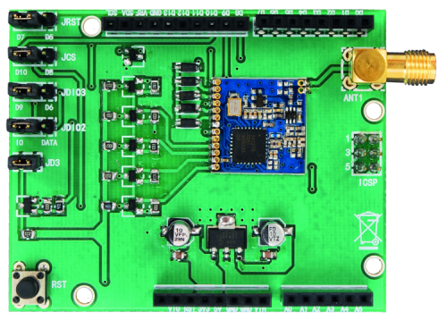
The RTCC shield has a double socketing that enables the insertion of the desired board, from time to time. After having described the firmware so to couple it to Arduino, in this last installment we will show you how to use our RTCC shield along with Raspberry Pi 2.0/B+, by taking advantage of the library that has been coded in Python and developed for this occasion. Before proceeding, we will summarize some of the details of the shield, that is based on the MCP79410 integrated circuit by Microchip; in particular, we will take a look at the interconnections between it and Raspberry Pi. Different lines are connected to the said board, among which the I2C communication bus for the management of the U1 integrated circuit (between Raspberry Pi and the U1 integrated circuit a level translator – that we better described in the first installment – has been interposed, since Raspberry Pi operates at a +3,3V voltage level, while U1 works at a level of +5V), the lines of the P1, P2 and P3 buttons, the trigger lines, the LED and the ON forcing line. If needed, the I2C bus (besides being brought to the U1 integrated circuit) may be extended –  by means of the usual expansion connector – towards other boards that are connected to Raspberry Pi: the important thing is that there is no overlapping with the hardware addresses that have already been reserved. Therefore, and in summary, the following Raspberry Pi’s pins have the following use:

  • the GPIOs 2 and 3 are used in order to connect the I2C bus;
  • the GPIOs 17, 18 and 27 are used in order to connect the three buttons that are used by the sketch that has been coded in Python;
  • the GPIOs 22 and 23 are used in order to connect the two trigger lines that are used during the debug stages;
  • the GPIO 24 is used in order to manage the ON forcing line of the electronics, by means of the Q6 NPN transistor and the corresponding Q1 MOSFET, that is used as a switch;
  • the GPIO 25 is used in order to drive the LD5 LED.

The description of the hardware made available by our board ends here, if you deem it appropriate to deepen your knowledge of the subject, we invite you to read the previous installment for more details.


THE LIBRARY FOR RASPBERRY PI

The library that we developed allows to configure and manage the MCP79410 in all its functions, so to make it easy to configure it for your needs, that may differ from ours. 

Differently from what in the Arduino world, the library has been written in Python and is composed of two files only, having the “.py” extension.

The first one is named “MCP79410.py” and contains all the library functions, while the second one is “MCP79410_DefVar.py” and contains the declarations of all the constants and data structures. The two files are therefore part of a package that may be installed in your Raspberry Pi and used for your sketches. We will see later how the package to be distributed is generated, and how to do to install it inside of your distribution.

In addition to the two library files, we wrote a sketch, so to show how to use the implemented functions. The sketch is composed of three different files: “MCP79410_Main.py” in which the main file is found, “MCP79410_PrintFunc.py” in which all the functions for the printing to video of the data read by the MCP79410 integrated circuit are found and finally “MCP79410_SetRegisters.py”, in which all the functions for the configuration of the MCP79410 integrated circuit are memorized.

Let’s start by broadly describing the “MCP79410_DefVar.py” file that, as above said, contains all the definitions of all the used functions, in addition to the declarations of the variables and of the public and private data structures. At a first glance it is possible to see that it is an almost identical copy of the corresponding file that has been created for Arduino, with some differences that are due to the programming language that has been used. 


dsc_0968


In the beginning of the file there are the declarations of constants, such as for example the integrated circuit’s hardware addresses (we would like to point out that the MCP79410 has two different hardware addresses), or the addresses of the registers for the reading/programming of the operating parameters of the IC. A series of constants for the programming of the registers with standard values follows; this section, if associated to the careful reading of the data-sheet, helps to fully understand what to configure and how to do it, for the purpose of the correct functioning of the integrated circuit. All of the constants that have been inserted may be modified at leisure by the user, according to his needs; for each constant there is a comment, whose purpose is to help to understand the meaning of the constant.

Finally, the constants for the management of the EEPROM find place; we would like to point out that in order to access it, the hardware address to be used is different from the one of the RTCC. In addition to the constants we just described, there are the data structures that are essential for a nested management of the data for the programming/reading of the different registers found.

The data structures are divided in different sections, in particular there are: a section for the TimeKeeper, a section for the alarms and a section for the TimeStamps. Similar to Arduino, it is possible to configure the registers in two different ways: a method considers the usage of specific dedicated functions, while the other one works by means of the configuration of the data structure and following programming of the registers. For example, the following data structure enables to configure every single bit in the “CONTROL” register:


class CtrlBit(Structure):
_fields_ = [(“SquareWaveFreqOutput”, c_uint8, 2),
(“CoarseTrimEnable”, c_uint8, 1),
(“ExtOscInput”, c_uint8, 1),
(“Alarm0_Enable”, c_uint8, 1),
(“Alarm1_Enable”, c_uint8, 1),
(“SquareWaveOutputEnable”, c_uint8, 1),
(“LogicLevelOutput”, c_uint8, 1)]
class CtrlByte(Structure):
_fields_ = [(“Byte0”, c_uint8)]
class CtrlReg(Union):
_fields_ = [(“ControlBit”, CtrlBit),
(“ControlByte”, CtrlByte)]


If we suppose we want to enable the alarm 0, we will have set the “Alarm0_Enable” bit, by means of the following syntax: 

MCP79410._CtrlReg.ControlBit.Alarm0_Enable = 1;


with “_CtrlReg” being the global declaration of the examined data structure, as shown by the sketch. Obviously, by acting like this we only set a value in the RAM. The next step is the one to recall a specific function in order to write a piece of data in the indicated memory location. For example, by using the “WriteSingleReg” library function, to which a series of parameters must be given, among which are the address and the value of the register whose value we wish to modify.

The complete syntax will be: 

mcp79410.WriteSingleReg(RTCC_HW_ADD, CONTROL_ADD,
MCP79410._CtrlReg.ControlByte);


In addition to the data structure we just showed, other and more articulated ones follow, they allow the configuration of the TimeKeeper registers, of the alarms and the reading of the TimeStamps at the PowerUps and at the PowerDowns.

As an example, let’s see the data structure as for the management of the TimeKeeper registers, as already seen for Arduino. Please notice the difference in the formulation of the Python code (used for Raspberry Pi) in comparison to the C code used for Arduino: for each register of the TimeKeeper two data structures have been defined, followed by a “union” so to allow access to the single register, both at a byte level and at the single bit level; on the subject, you will see the first data structure highlighted in yellow, it concerns the setting of the seconds plus the oscillator’s activation bit; other data structures follow and they are highlighted in grey.


fig_1


Among these sections, eight are needed just for the management of the TimeKeeper’s registers.

All of the eight sections are then grouped together in another data structure, so to have a single structured access to the registers (the section is highlighted in green). With this approach there is a single “container” from which it is possible to modify a single bit or a whole byte of the registers that are related to the TimeKeeper.

In order to better clarify the idea, we will give some examples, let’s suppose we want to set the “StartOsc” bit of the “RTCSEC” register: 

MCP79410._TimeKeeper.Seconds.SecBit.StartOsc = 1


in which “_TimeKeeper” is the global declaration of the data structure being examined, as shown in the sketch.

If – on the other hand – we wanted to set the “VbatEn” bit, for the purpose of enabling the battery management of the integrated circuit, we will have to proceed as follows: 

MCP79410._TimeKeeper.WeekDay.WkDayBit.Vbaten = 1


Once the registers of the above described data structure have been configured, it is possible to proceed with the actual programming of every single register of the integrated circuit, by taking advantage of the “WriteSingleReg” library function, to which three parameters must be given (hardware address, register address and value to be written in the register); or it is possible to proceed with the complete programming of all the TimeKeeper’s registers, by taking advantage of the “WriteTimeKeeping” library function, to which to give a single parameter, so to indicate if the hour management format is 12h or 24h. Therefore the syntax for programming all the registers all at once (with the 24h hour format) will be: 

MCP79410.WriteTimeKeeping(0)


The functions here made available by the library are the same ones of the corresponding one for Arduino.

We will therefore avoid to describe every single function but will limit ourselves to make a list, so to focus on the code and its functions. The full list is shown in Listing 1.

We would like to point out that the “ControlByte” variable identifies the hardware address of the I2C peripheral, in this case we have two addresses: one for the RTCC and the other one for the EEPROM; the “RegAdd” variable identifies the register address that we wish to read or write, the “Bit” variable indicates which bit of the desired register we wish to modify while “RegData” indicates the 8 bit value that we wish to write in the register.

The “SetReset” and “EnableDisable” variables are respectively needed in order to set or reset a function of the integrated circuit, or to enable or disable a function.

SetHourType” is needed in order to set the hour format (12H or 24H), “SetAmPm” is needed in order to tell if the indicated hour is before noon or after, “Alarm0_1” indicates on which alarm we wish to operate, while “Mask” is the masked comparison for the generation of an alarm trigger condition.

Finally, “PowerDownUp” indicates if we wish to read/write the registers, with the references to time and date that have been detected during the PowerUp or PowerDown stages.

Listing1

1) ToggleSingleBit(ControlByte, RegAdd, Bit)
2) SetSingleBit(ControlByte, RegAdd, Bit)
3) ResetSingleBit(ControlByte, RegAdd, Bit)
4) WriteSingleReg(ControlByte, RegAdd, RegData)
5) WriteArray(ControlByte, StartAdd, Lenght)
6) ClearReg(ControlByte, RegAdd)
7) ReadSingleReg(ControlByte, RegAdd)
8) ReadArray(ControlByte, StartAdd, Lenght)
9) GeneralPurposeOutputBit(SetReset)
10) SquareWaveOutputBit(EnableDisable)
11) Alarm1Bit(EnableDisable)
12) Alarm0Bit(EnableDisable)
13) ExternalOscillatorBit(EnableDisable)
14) CoarseTrimModeBit(EnableDisable)
15) SetOutputFrequencyBit(OutputFreq)
16) StartOscillatorBit(EnableDisable)
17) Hour12or24TimeFormatBit(SetHourType)
18) AmPmBit(SetAmPm)
19) VbatEnBit(EnableDisable)
20) AlarmHour12or24TimeFormatBit(SetHourType, Alarm0_1)
21) AlarmAmPmBit(SetAmPm, Alarm0_1)
22) AlarmIntOutputPolarityBit(SetReset, Alarm0_1)
23) AlarmMaskBit(Alarm0_1, Mask)
24) ResetAlarmIntFlagBit(Alarm0_1)
25) PowerHour12or24TimeFormatBit(SetHourType, PowerDownUp)
26) PowerAmPmBit(SetAmPm, PowerDownUp)
27) ResetPwFailBit()
28) WriteTimeKeeping(SetHourType)
29) ReadTimeKeeping()
30) WriteAlarmRegister(Alarm0_1, SetHourType)
31) ReadAlarmRegister(Alarm0_1)
32) WritePowerDownUpRegister(PowerDownUp, SetHourType)
33) ReadPowerDownUpRegister(PowerDownUp)
34) Set_EEPROM_WriteProtection(Section)
35) WriteProtected_EEPROM(RegAdd, RegData)


THE LIBRARY AS A PACKAGE

In order to facilitate the usage of the library, we created a distribution package, simply named as “package”. With such a measure the user installs the Python library that has been created on his Raspberry Pi, the latter is placed in a specific path on the disk, so to be recalled in your sketches by means of the “import” function.

In order to create a package you have to organize the code in the following way:

please create a base folder with a meaningful name. In our case it was “MCP79410”;

please create – inside of the above said folder – a new one, still having the “MCP79410” name, and inside of it please copy the two library files, “MCP79410.py” and “MCP79410_DefVar.py”.

please create an additional empty file in Python, having the “__init__.py” name; in this way the Python interpreter will see this folder as a distribution package (technically named as “package”);

in the base folder (please refer to the first step), please create the “setup.py” file, that must contain the following Python code lines:

from distutils.core import setup
setup(name = “MCP79410”,
version = “1.0”,
description = “MCP79410 Library”,
long_description = “This package is usefull
to manage the Real Time clock
Calendar MCP79410 developed
by Microchip”,
author = “Matteo Destro”,
author_email = “info@open-electronics.org”,
url = “www.open-electronics.org”,
license = “GPL”,
platform = “RaspberryPi”,
packages = [“MCP79410”])


Given that when a “setup.py” file is created, one always has to import the “setup” entry from the “distutils” library and to proceed at a later stage to compile some fields, in our case we gave a name to our distribution by means of the “name” entry, we highlighted the version by means of the “version” entry, we gave a short description by means of the “description” entry, followed by a more comprehensive description by means of the “long_description” entry. They are followed by the “author” entry and by the corresponding support e-mail address, “author_email”. The “url” entry follows, along with the link to the developer and the corresponding software “license”. Finally there is a “platform” entry, for which the code has been developed, and the “package” entry (so to identify that the one being considered is the distribution package). In order to create the distribution package the following command must be executed:

sudo python setup.py sdist


that creates a compressed file that contains the distribution package; the file that is created is “MCP79410-1,0.tar.gz”. Therefore the user that wishes to install the library will have – as a first thing – to decompress the file in a directory at leisure and then to execute the following command so to install the library:


sudo python setup.py install


In order to import and use the library in your sketches you will have to insert the following code lines in the beginning of your sketches:

import sys
sys.path.insert(0, “/usr/local/lib/python2.7/dist-packages/MCP79410”)
import MCP79410


AN EXAMPLE OF CODING

The code we just created has two different purposes: the first one is to show you how to use the available library, in addition to the procedures for the configuration of the registers of interest; the second one is the one to explain you how to interact with the hardware of our demo board, since the objective is to automatically turn on and off Raspberry Pi, under certain conditions that have been dictated by how the alarm registers have been configured.

Let’s start the explanation from the main file, that is to say, the one containing the “main()” routine.

Please notice that in the beginning of the file there are the famous code lines with the “import” instructions, so to include the library we just talked about, in addition to other system libraries that are needed. 

Soon after they are followed by the declarations of the global variables, by the declarations of the constants that identify the GPIO pins that have been used and their configuration as inputs or outputs. As inputs there are only the P1, P2 and P3 buttons, to which an internal pull-up is imposed, plus an event on the falling edge, with a debouncing time of 100 milliseconds, so to intercept the pressure of the button.

We prepared two timers, so to read with the registers of our MCP79410 we are interested in, at regular intervals; one has  an interval of 5 seconds (def ReadsAndPrintsRegisters():) and the other one has an interval that is equal to 1 second (def CheckAlarmsFlag():).

With an interval that is equal to 5 seconds, the TimeKeeper’s registers are read (for the purpose of showing the current date and time), as well as the the alarm registers (so to view their configuration) and, if needed, the TimeStamp registers. The latter are read only once when starting our Raspberry Pi board.


dsc_0966


The second timer, set with an interval that is equal to 1 second, is needed in order to monitor the alarms; in the case one of the two alarms is active, one of the two following actions will be executed:

Action concerning the board’s planned switching on. Alarm 0 is set so to switch on our board’s electronics at a certain time, and consequently, Raspberry Pi as well.
Therefore, in this case the sketch will detect that alarm 0’s flag is at 1, it forces the power source to ON by means of the “FORCE_ON” line and resets the alarm flag.
Before ending the process, it disables alarm 0 and activates alarm 1.

Action concerning the board’s planned switching off. Alarm 1 has been set so to force Raspberry Pi’s switching off and therefore the one of our electronics as well, at a certain time. In this case the sketch detects that alarm 1’s flag is at logic 1 and consequently it enables alarm 0 and disables alarm 1, it resets alarm 1’s pending flag and sends the shutdown command to Raspberry Pi, which will start its switching off procedure. Once the Raspberry Pi shutdown is completed, the “FORCE_ON” line will be released, with our electronics consequently switching off. 

Each one of the two timers we examined is a “thread” and in order to start them the following code line must be used: 

threading.Timer(1.0, CheckAlarmsFlag).start()


in which the first parameter indicates the interval – 1 second in this case – while the second parameter indicates to which function it is associated. The first start simply occurs by recalling the “CheckAlarmsFlag()”  function from the main file, before entering the infinite loop.

More in detail, we will now see the code found in the two timers: for example, the one in “CheckAlarmsFlag()”. You will notice that our MCP79410 library is recalled more than once, be it at a reading level as for the data structure only, or at a call functions level. For example, the flags of the two alarms are tested by taking advantage of the data structure: 

if (MCP79410._Alarm.Alm[0].WeekDay.WkDayBit.AlarmIF == 1):


This data structure is a structure array, since the alarms are two. In the code we presented, it points to alarm 0, and in particular to the WeekDay register (ALM0WKDAY) and to the related alarm flag (ALM0IF). Please refer to the data-sheet for the details concerning the registers. In addition to the test we presented before, there are some call functions, such as, for example, “MCP79410.Alarm0Bit(0)” which is used so to reset alarm 0, or “MCP79410.ResetAlarmIntFlagBit(0)” which is used so to reset the flag for alarm 0.

Now, let’s analyze the “main()” routine: in the beginning, a reading of the EEPROM that is internal to the MCP79410 is executed (exclusively for educational purposes), and in order to do so it takes advantage of the library function used in order to read a byte array, starting from a given address. The function has three parameters: 

MCP79410.ReadArray(MCP79410.EEPROM_HW_ADD, 0, 13)


The first one is the hardware address that (as already said it is different from the one of the RTCC) follows the starting address from which the data reading begins, and finally the number of bytes we want to read. The result from the reading is put into an array to which the following one points: 

MCP79410.DataArray[i]


in which “i” is the array address. The maximum size is set to 16 byte. The content is then printed to video and it makes the “ElettronicaIn” writing appear. Writing in EEPROM has been carried out by means of the function with the same name: 

MCP79410.WriteArray(MCP79410.EEPROM_HW_ADD, n, m)


to which to give the same parameters given to the previous one. The activation of the two timers (we talked about them before) follows, and finally there is the infinite “while” cycle.

Inside of the “while” loop the management of the three buttons, P1, P2 and P3, takes place; three different functions have been assigned to them.

The P1 button is used in order to program MCP79410’s time and date, and to do so it recalls a specific function that reads the system’s time and date and transfers them to the integrated circuit. The function that deals with MCP79410’s time and date is named “SetTimeKeeperByLocalDateTime(“24H”)” to which only a parameter must be given, that is to say, if the hour format has to be 12h or 24h. The parameter is of the string type (the function is memorized in the “MCP79410_SetRegister.py” file). If, on the other hand, you want to manually set time an date, the following function must be recalled: 

ManualSetTimeKeeper(Hours, Minutes, Seconds, Set_12H_24H, Set_AM_PM, Date, Month, Year, WkDay)


which requires a series of parameters. A practical example could be the following one: 

ManualSetTimeKeeper(15, 30, 00, “24H”, “AM”, 25, 12, 15, 5)


In this way the hour is set to 15:30:00 in the “24H” format, the date is Friday, 25/12/2015, and the “AM/PM” indication, has no more meaning.

Were it in the “12H” format, we would have had to give the parameters in the following way: 

ManualSetTimeKeeper(03, 30, 00, “12H”, “PM”, 25, 12, 15, 5)


In both cases the functions fill the data structure concerning the TimeKeeper’s registers, and then they recall the library function that physically writes on the device.

The P2 button is used in order to program the alarms 0 and 1; for the purpose it recalls two different functions, one for alarm 0 and the other one for alarm 1.

The configuration is only of the manual kind and is only executed from the code; this means that we didn’t prepare a system to enter data from the keyboard. The function to be recalled in order to set the alarms is the following one: 

ManualSetAlarm0(Index, Hours, Minutes, Seconds,
Set_12H_24H, Set_AM_PM, Date, Month, WkDay, AlarmMask, AlarmPol)


As you may notice, there are many parameters to give to it; an example could be:

ManualSetAlarm0(0, 12, 40, 00, “24H”, “AM”, 25, 12, 1, 1, “LHL”)


In this way we are telling to the function to work on the alarm 0, the hour is in the “24H” format and set to 12:40:00. The date is set to 25/12/****. The year has not been specified, since it is meaningless for the alarms. The day of the week is Monday, the mask for the alarms has been fixed at the minutes, the polarity is “Logic High Level”.

Even in this case, the function fills a data structure, and then recalls a library function that physically writes on the device. We suggest to check the data-sheet for the details concerning the registers.

The P3 button is used in order to disable and reset the alarms 0 and 1. After that the alarms have been reset and disabled, the sketch limits itself to showing the time and date read by the RTCC, with an interval of 5 seconds.

As for the printing to video of such information, the printing function contained in the “MCP79410_PrintFunc.py” file is recalled; a series of parameters must be given to it, in order to decide what to print and what not.

The function being examined is named like this: 

PrintDataMCP79410(PrintTimeKeeper, PrintAlarm0, PrintAlarm1, PrintPowerDown, PrintPowerUp)


The parameters to give are just boolean values -true or false- and tell the function what to print to video.

As suggested by the names, we have the following sequence:

  • printing to video of time and date;
  • printing to video of Alarm 0’s settings;
  • printing to video of Alarm 1’s settings;
  • printing to video of the TimeStamp PowerDown values;
  • printing to video of the TimeStamp PowerUp values.

If all the boolean values are set to “False”, nothing will be printed to video.


AUTOMATIC SKETCH START AFTER THE BOOT

The next step consists in making our code a self-booting one, after that the operating system’s boot has taken place. For the purpose, as a first thing we have to decide if to keep the login active or not; in the case in which we decided to skip the login stage, you have to proceed like this:

sudo nano /etc/inittab 

2) search for the following line in the file:

1:2345:respawn:/sbin/getty –noclear 38400 tty1


3) comment it by using the “#” character at the beginning of the line; and add the following one (“pi” is the username) under it:

1:2345:respawn:/bin/login -f pi tty1</dev/tty1>/dev/tty1 2>&1


4) exit and save the thus modified file by pressing “ctrl+x” and after that, “y”;

5) once the file has been saved, please execute the following command:


sudo nano /etc/profile


6) go to the end of the file and add what follows:


sudo python /home/pi/PythonProject/MCP79410_Lib/WK/MCP79410_SetAndReadRegisters.py


Obviously, you will have to use your system’s path; in our case the path in which the three files of our sample sketch are found is “/home/pi/PythonProject/MCP79410_Lib/WK/”. Finally, restart the system.


CONCLUSIONS

With this, we ended the discussion concerning the management of our board, supplied with the RTCC, via Raspberry Pi. We gave some food for thought, so that you may create your diverse applications by taking advantage of our Python library, that we purposely wrote for this occasion.

All that is left is to wish you good work!


How to configure Raspberry Pi

If this is the first time that you are using Raspberry Pi or if you never tried to write some code in Python, it is appropriate to execute a series of steps in order to configure Raspberry Pi, so to use the management libraries of the GPIOs and of the I2C bus. Let’s see how to proceed, step by step:

As a first thing, please install the Python library for the management of Raspberry Pi’s I/Os and, if already installed, please update it to the last available release, that is currently 0.5.11.

  • In order to verify the current GPIO library version, please execute the following command:


find /usr | grep -i gpio 


Figurehighlights the feedback as for the sent command, in this case the library turns out to be updated to the last release. If the library release is older than the 0.5.11, please update it by using the following commands: 


sudo apt-get update

sudo apt-get upgrade 


figura-2


or by giving the following ones:


sudo apt-get install python-rpi.gpio

sudo apt-get install python3-rpi.gpio


Let’s move on to the configuration of the I2C peripheral, that is made available by Raspberry Pi:

  • let’s proceed with the installation of the “smbus” Python library for the management of the I2C bus:


sudo apt-get install python-smbus 


  • followed by the one for the I2C tools:


sudo apt-get install i2c-tools


We will then have to enable the I2C bus support on the part of the kernel; in order to do so it is needed to recall the configuration window, by typing in the following command:

sudo raspi-config


  • as in figure, let’s select the “Advanced Options” entry;
  • in the new window, let’s select the “A7 I2C Enable/Disable automatic loading” entry;
  • in the following screens, please answer “Yes”, “Ok”, “Yes” and finally again “Ok”;
  • let’s exit from the configuration window by selecting the “Finish” entry;


figura-3

figura-4


Let’s proceed with a system reboot, by executing the following command:


sudo reboot


  • after having restarted Raspberry Pi, please open the “modules” file by means of a a general text editor;

sudo nano /etc/modules


  • please add – if they are missing – the two following lines, as highlighted by figure.


i2c-bcm2708

i2c-dev


figura-5 


Lastly, you will have to verify the following file in your distribution:

/etc/modprobe.d/raspi-blacklist.conf


  • Should it be there, please open it by means of a text editor:

sudo nano /etc/modprobe.d/raspi-blacklist.conf


  • Should they be there, please comment the following lines, by using the “#” character:
    blacklist spi-bcm2708

blacklist i2c-bcm2708


At this stage, all that is left is to restart again Raspberry Pi, and to verify that the I2C communication is active. In order to do so, please execute the following command:

 sudo i2cdetect -y 1


If everything reached a successful ending, the command sent will return a table like the one shown in figure. In practice, the command analyzes the I2C bus, looking for peripherals, and in our case it found the MCP79410 integrated circuit, along with its two addresses, 0x57 and 0x6F.


figura-6


From openstore

Shield RTC for Raspberry e Arduino

Arduino UNO R3

Raspberry Pi 3 Model B with Wi-Fi and Bluetooth

The BF 15+15W open source power amp

$
0
0

featured


A compact stereo amplifier that may be used at home as well as in the car, and also to substitute broken audio power amplifiers or to create bench power amps for the analysis of audio devices.

When repairing audio devices, it is always useful to have a BF amplifier on your workbench; all the better if it is a stereo one, since with such an amplifier it is possible to test stereo devices such as Compact Disc readers, cassette decks, tuners, MP3 readers and so on. Therefore we designed a very compact amplifier for the lab (and not just that), a proposal for you so that you may create it. It is composed of very few elements that surround the monolithic integrated circuit by ST, that is capable of supplying an output power of 2×15 watt, that are effective on a 4 ohm load (speaker). A good output power and good sonic qualities (as regards the harmonic distortion and the bandwidth) allow to make the circuit a suitable one even for applications that have nothing to share with the lab: for example, it is possible to use it as a power amplifier for a pair of amplified speakers for the PC (the amplifier is placed into one of them, the other one is connected by means of a flat cable) or a self built stereo system. The amplifier may even be used for the substitution of the broken power amp of a compact hi-fi system for which it is no longer possible to find the spare parts, because of its very small size and good performances as regards the sonic quality. In fact it is an amplifier that without doubt may be placed among the high fidelity ones. But we will talk about the applications later, after an overview of the circuit diagram and after having analyzed its functioning and features.


dsc_0953


Circuit diagram

The amplifier revolves around a monolithic integrated circuit for universal use, that is composed of two BF amplifier stages having a bridge output, that may be equated to operational amplifiers connected by a bridge and supplied with a low impedance output stage; each stage has a fixed voltage gain that is internally set by the retroaction resistors (they are quite accurate and guarantee a maximum gain difference, between the right and the left channel, of just 0.5 dB) of these operational amplifiers, that is equal to 32 dB, corresponding to about 39 times the original signal. This means that by supplying an effective voltage of 0.1 V as an input, we obtain 3.9 V as an output. The maximum output power with a 8 ohm speaker is 15 watt, in order to obtain them we need an effective voltage of 10.9V; since the voltage gain is 39 times the original signal, in order to obtain such a power it is needed to drive each stage with 0.28 Veff. In order to obtain the same power at 4 ohm, since we need a voltage on the load that is equal to 0.707 times the one required on 8 ohm, 198 mVeff are needed as an input. Anyway, please pay attention to the fact that for each channel, the TDA7297 may supply a peak current of 2 ampere, and under a sinusoidal regime that means a bit more than 1.4 ampere; this value is more than enough to supply 15 watt at 8 ohm, but it allows to reach a maximum of 8 watt at 4 ohm; it is therefore possible to connect 8 ohm amplifiers, but the power obtained is less than the one obtained at 8 ohm.


1240_schema


Only very few external components are needed by the integrated circuit, since internally it has everything it needs: the polarization networks of the operational amplifiers’ non-inverting outputs, that are needed since the integrated circuit is powered with a single voltage, the R/C series networks (Boucherot cells) in order to compensate the impedance variations of the speakers and to prevent the self-oscillations, in addition to the bootstrap networks that are needed for the purpose of stabilizing the polarization when the component is started.

This makes the diagram a very simple one, as you may see from these pages: in fact the integrated circuit is surrounded only by two capacitors for the uncoupling of the L and R inputs (C4 and C5) in the direct current, and by a resistive voltage divider, in addition to a filter capacitor for the inputs of the Mute and Standby functions; more specifically, the C3 capacitor allows – when the circuit is started – to silence the outputs of the amplifiers, so to avoid the classic “bang”, due to the initial adjustment of the polarization networks; it is better to prevent it, because it is both annoying and a strong stress for the speakers, and specially for the low frequency sigmals. The Mute function is activated by setting the pin 6 to logic zero, as for the Standby function it is activated by setting the pin 7 to level zero, therefore we are able to manage both of them with a single network; as an effect of the capacitor, that is uncharged when the circuit is powered, initially the power stages are switched off and the Mute blocks the audio signal for a time that is equal to about 100 milliseconds, once they have passed it lets the TD7297 to operate normally. The capacitor is discharged by means of the R2 resistor, and once it is switched off (that is to say, when deprived of power) the circuit is discharged via R3; if there wasn’t such a resistor, the load would remain for a long time and at a following close restart it would not allow the activation of the Mute and Standby functions.


collegamenti


The manufacturer advises to switch the TDA7297 on, only after having deactivated the Standby and then the Mute function, in this order. Since the deactivation threshold of the Standby function is 0.9 volt (therefore, when the voltage suppllied by the C3 capacitor grows to 1 V, the integrated circuit goes to full speed) and the one of the Mute function is about 2.9 volt, the connection that we created is fine, in the sense that we may use a single RC network in order to drive the command pins for both functions, being sure to respect the correct starting sequence. The single network is fine for the switching off as well, since ST recommends to set the integrated circuit to Mute and then in Standby mode, and this is respected as well, since as the voltage drops on the capacitor, the Mute is first activated, and then the Standby mode, too.


pinout


The integrated circuit’s outputs are directly connected to the speakers: even though the circuit operates with a single voltage, no uncoupling capacitors are required, since the speaker of each channel is connected between the outputs of the two power stages of the corresponding channel.

Each input has a potentiometer (actually a cross-section of a dual potentiometer) in order to measure out the signal’s level that reaches it and therefore to obtain the control of the volume, it reaches the maximum when the pointer is found towards the IN contact, and it reaches the minimum when it is at ground.

On the power source line, the C1 and C2 capacitors have been located; they have the purpose to filter both the pulse disturbances and the possible ripple of the power source that has been used, and the voltage fluctuations caused by the absorption variations on the part of the integrated circuit at high output power levels. The presence of power voltage (that in order to obtain the maximum power at 8 ohm must be of about 16.5÷17 V), is signalled by the lighting up of the D1 LED, that is polarized by means of the R1 resistor.    


Power amp usage

As for the applications, the circuit may be used – in addition to the usage as an amplifier for fixed applications (as bench power amp, hi-fi amplifier) – as a small booster for car radios that are not supplied with an amplification: it is excellent, for example, for the purpose of amplifying the signal provided by a MP3 reader.

Whatever will be the way you are going to use it, please keep in mind that the container or housing in which you will place it must have wide openings, so to allow the TDA7297’s dissipator to dispose of the heat produced by the integrated circuit; please avoid the dissipator to touch possible metal parts of the container or housing, since even though the metal winglet is connected to ground, it is always better to avoid parallel paths to ground, that may create interferences that could be heard through the speaker.

In order to limit the interferences, such as for example the buzz induced by the 220 V electric network, it is useful to enclose the circuit in a metal container; as for the ventilation, you may have the dissipator to come out from a small window, or to consider the idea of creating some grids. Please remember to connect to ground (of the power source) in a single point of the container, and to insulate the metal part of the input connectors (please use the RCA) from the container, even if – from an electrical point of view – it goes to the circuit’s ground.


blocchi


TECHNICAL FEATURES

  • Power voltage: 7÷18Vcc
  • Output power (RMS): 15+15 W   at 8 ohm
  • Output power (RMS): 8+8 W   at 4 ohm
  • Max current drawn: 2.5 A
  • Current drawn at standstill: 50 mA
  • Frequency response:    22Hz÷100 kHz
  • Harmonic distortion (@1W): 0.1 %
    Harmonic distortion at the maximum power: 1 %
  • Channel separation: 60 dB
  • Input impedance: 30 kohm
  • Thermal protection
  • Protections from outputs short circuiting


From openstore

Audio Amplifier Module 2 x 15 watts

A Christmas Star with Neopixel LEDs

$
0
0


A tech Christmas decoration, created by means of Neopixel LEDs and controlled via an Arduino Micro board, that takes up a minimal amount of space.

With the Xmas holidays approaching, we always try to propose a solution or another, one that is capable of combining tradition and innovation, so to avoid the usual or the trivial – even if always welcome – gadget, that is used as a Christmas decoration: and they cannot be missing from the Christmas tree, the window and the doorstep. For such matters, RGB LEDs and light strips have become a must-have and therefore we could not exempt ourselves from proposing a classic light decoration (the more lights there are for Christmas, the better, as they are a symbol of life and hope…) that has been reconsidered in a modern key, since it has been entrusted to the adaptable and powerful Neopixel LEDs. With a certain amount of the latter, that have been connected in queue and managed in cascade by an Arduino board, we gave life to a 5-star Christmas star, that will show-off at the top of the tree, or wherever you might want to place it (as an example, at the doorstep).

Let’s see therefore what it is all about, by analysing the circuit diagram, that is made of a part that is composed by the LEDs and the control board, that in our case is an Arduino Micro, just for the purpose of minimizing the amount of space occupied by the star.


Circuit diagram

Let’s take a look, therefore, at the project’s electrical section, that is essentially composed of a set of 56 Neopixel LEDs, that have been arranged so to form two concentric stars; the first 35 RGB LEDs (out of 56) form the bigger, external star, while the other 20 ones form the smaller and internal star. The LED number 56 is placed exactly at the center of the printed circuit board, that has the shape of a five-pointed star.

The Neopixel LEDs are connected in cascade but powered in parallel; such a configuration enables to address each single LED and to individually choose the colour; among the possible hues, the 256 possible combinations for each primary colour (therefore we have 256x256x256 combinations!) determine a total of 16,777,216 colours: that’s what one would call true colours!


Neopixel provides you with the integration of a driver for each RGB LED and therefore of a LED by LED driving capability. The data channel for the communication is of the serial, oneWire kind, and the power source is a 5 volt one; the Neopixel LEDs are connected in cascade, meaning that the input data line – in addition to reach the corresponding controller – is repeated at the output.  The communication on the data channel is carried out at a maximum of 800 kbps and is of the type having an embedded clock. The serial control is indispensable since otherwise – in order to individually manage the single LEDs that form our star – we would need a lot of lines, even if adopting a multiplex matrix command. On the contrary, we need a single data channel, to be managed by means of a single line of the Arduino board, for reasons of simplicity and space occupied. The solution we adopted allows to rely on a very small Arduino Micro, while if we had to implement the multiplex for our 56 LEDs, the amount of lines would have forced us to adopt the “big ones” of the Arduino family.


While it is true that the LEDs of the Neopixel system may be connected in cascade, so that the data line from one goes to the next one, the collateral effect is that – after a certain amount of LEDs – the management speed must be considerably reduced; because of that, if we have to create matrices in order to show some quick graphic artwork, it is better to use many lines with just a few LEDs for each one; this is not our case, however, since for our Christmas star, even though some animations determines a variation of the individual brightness in order to compose the various light effects, the execution speed for the games is such to not reach the data-rate limit for the Neopixels.

The implementation of all the “effects” is available on Listing 1.

Listing1

void startShow(int i) {
Imposta_Colore(modo);
switch(i){
case 0: colorOff(); //Off
break;
case 1: Imposta_Colore(random(0,colore_max));
Stella1_Dissolvenza(); //Fade star 1
Stella2_Dissolvenza(); //Fade star 2
break;
case 2: Stella1(); //Star sequential switch 1 and Off
Stella2(); //Star sequential switch 2 and Off
break;
case 3: Stella_Alternata(); //alternate lighting stars
break;
case 4: Imposta_Colore(random(0,colore_max));
for (int ciclo=0; ciclo<3; ciclo++)
{
colorCarica(); // charge effect
delay(pausa_effetti*2000);
colorScarica(); // discharge effect
delay(pausa_effetti*1000);
}
break;
case 5: Stella_Casuale();
break;
case 6: Imposta_Colore(random(0,colore_max));
Strobo(); // Effect strobo
break;
case 7: Imposta_Colore(random(0,colore_max));
barraScorrevole(pausa_sfumatura); //scrolling effect
break;
case 8: rainbowCycle(12);
break;
case 9: colorMix (10);
break;
}
}


If you’d like to apply some modifications to the firmware, in order to create some effects that have not been designed by ours (Listing 2 shows a sample one, that deals with the fade-in start for the two stars…), please remember that the refresh frequency – and therefore the switching on/off speed as for the single LEDs – is inversely proportional to the amount of LEDs to be managed.


For each LED strip, it is possible to set the refresh frequency at leisure, so to make some tricks of the light imperceptible. In our case, the scan frequency for the LEDs is 400 Hz. The maximum data sending speed influences – the number of commandable LEDs being equal – the refresh frequency; this means that the more the LEDs to be managed, the less the refresh frequency and so the moving speed of the picture shown.

Listing2

void Stella1_Dissolvenza(void)
{
int pixel = 0;
int i=0;
uint32_t R=0;
uint32_t G=0;
uint32_t B=0;
num_pixel=strip.numPixels(); //get the number of pixels (LEDs)
colorOff(); //Off
for (int ciclo=0; ciclo<7; ciclo++)
{
if (R_ON==true) R=0;
if (G_ON==true) G=0;
if (B_ON==true) B=0;
//Increase brightness
for(int i=0; i<luce_max; i++)
{
if (R_ON==true)
{
R=i;
}
if (G_ON==true)
{
G=i;
}
if (B_ON==true)
{
B=i;
}
for(pixel=0; pixel<num_pixel-21; pixel++) //turn on the first star in a gradual manner
{
strip.setPixelColor(pixel, strip.Color(R, G, B));
}
strip.show();
delay(pausa_sfumatura/2);
}
//decrease brightness
for(int i=luce_max; i>0; i--)
{
if (R_ON==true)
{
R=i;
}
if (G_ON==true)
{
G=i;
}
if (B_ON==true)
{
B=i;
}
for(pixel=0; pixel<num_pixel-21; pixel++) //It updates the status of the first star
{
strip.setPixelColor(pixel, strip.Color(R, G, B));
}
strip.show();
delay(pausa_sfumatura/2);
}
}
}

The command protocol of the Neopixel system provides a cyclical sending (at a frequency depending on the one of the desired refresh) of data strings, each one is composed of 24 bits, divided in groups having three bytes each (therefore, 3×8 bits); each one of the bytes of a 24-bit string contains the lighting state for each primary colour, in this order: first the eight bits for the green colour, then the ones for the red and finally the ones for the green. In the circuit diagram, the connection in cascade of the Neopixel LEDs is shown: the data line entering the DI terminal exits from the DO one, that repeats its data; the DI of the first LED (LD1) refers to the IN contact of the circuit, to which the data supplied by Arduino is applied. The reference ground for the power source and the data is a single one and refers to the GND contact of the printed circuit board; the 5 volt power source, too, and refers to the 5V contact. With reference to the wiring diagram, we may see that Arduino drives the star’s circuit by using the data line only, therefore the IN contact is connected to the said I/O of the board, that is the digital pin 9, that in this application has been set as an output in the sketch. The star’s power is drawn from Arduino Micro’s 5V and GND lines; for obvious reasons regarding the absorption, the Arduino board must be powered by an external power source, one that is capable of supplying about 800 mA (stabilised) on the 5V. It is possible to obtain the power from the microUSB socket or to supply it between Vin and GND, but in this case the power source will have to supply at least 7 volts.


Practical implementation

Let’s move on now to the building of our star, that requires a double sided printed circuit board, that may be obtained via photoengraving, by starting from the tracks on the bottom-side that you will find on our website, along with all the other files of the project. Once it has been engraved and drilled, the PCB (we will start from a double-sided board having a size that is such to host a star) must be processed, by cutting it and smoothing it down by means of coarse or medium sand paper, so to give it its definitive shape for a 5-pointed star.

Once this has been done, it is possible to mount the Neopixel LEDs and the capacitors, to be placed as shown in the assembly diagram that you will find in these pages; the components are SMD ones, exception made for the connector having the 90° pins, that must be mounted lastly, on the opposite side of the one where the LEDs and the capacitors are placed. The creation requires a bit of dexterity and practice with the SMDs; therefore please acquire a fine tip soldering iron, some solder wire (having a maximum diameter of 0.5 mm), some flux paste (one that has low density) and a small brush so to spread it, in addition to tweezers (so to handle the components) and a magnifying glass (so to verify – as a first thing – that they have been correctly placed and then correctly solded). It will be useful to have some desoldering braid, so to remove some excess tin that may shortcircuit pins or pads.

Mounting the connector does not create any problem: it is enough to insert the terminals in the corresponding holes and to solder them from the side where the components are found. In order to connect Arduino Micro you will have to use some jumpers whose ends you will have to cut, in order to solder them to the contacts of the detached female connector that you will insert in the star’s 3-poles plug; please remember that the ground (GND) goes on the middle contact, the data IN to the external side of the star and the 5V in the internal one. Before connecting Arduino, you will have to connect it to the PC by means of a USB/microUSB cable and to load on it the sketch you will find available for the download at our website, along with the project files. Once the firmware has been loaded, and the whole has been connected and powered, you will be able to verify that everything works properly: the animations should start a few moments after having supplied the power, since the sketch we have written allows to generate different effects that are sequentially cycled, as soon as the power has been supplied.


Please notice that if you power everything from the Vin and GND pins of the Arduino board, you must not leave the computer connected to the USB.

From openstore

FT1300M – CHRISTMAS STAR WITH LED NEOPIXEL


Print with Chocolate in two colours with 3Drag Choco Big Dual Extruder

$
0
0


Let’s create a new evolution for our 3Drag printer, with a dual extruder for the printing of chocolate items of two types or colours.

The 3Drag printer has been our answer to the growing need – on the part of the general public (a need that was already shown towards the RepRap project) – for an open, affordable and customizable 3D printer; it’s not by chance that this printer, born in the summer of 2012, gained fame as the “most hackable 3D printer in the world” in a short time. And this because it was born out of a completely open project. We showed that in time, by showing you how it may become a CNC milling machine, and also a printer of chocolate items. We then “stretched it out” so to have it print items having a greater size: and so the 3Drag Big was born. But the requests for the expansion of this project follow one another unrelentingly; those who tried the Choco printer kit showed their will to print chocolate items having more colours, or using different kinds of chocolate in a single step; from here the idea of creating a 3Drag Choco with dual extruder was born: we will describe it in this article.

Certainly, to create it wasn’t a task as immediate as designing it, since, given the size of the printhead, in order to mount two of them (with the power source mechanism as well) we had to keep the nozzles at a distance that could be compared with the one on the side of the build plate; therefore, in order to cover the same printable size, it became necessary to increase the print head’s travel on the side of the direction on which the extruders are aligned, and therefore to resort to the 3Drag Big’s structure, that has a longer plate.   

Moreover, we had to review the electronic parts, since in order to drive two extruders, the single controller board wasn’t enough anymore.

We won’t publish the circuit diagrams and the assembly instructions of the 3Drag printer again, and we refer you to the corresponding articles; in these pages we will describe the modifications that are needed in order to transform the 3Drag BIG in a 3Drag BIG DualChoco. Those who already have a 3Drag will be able to find the instructions for its transformation in a 3Drag Big (that will be the starting point) at the following web page: 3DRAG BIG

The procedure that has been described in these pages has been perfected during the lab educational activities of the course of Industrial Automation, taught by the Department of Industrial Engineering of the University of Parma, and of the course in Systems for the Automated Production, taught at the SUPSI (Professional Universitary School of the Italian Switzerland); a cooperation between the two universities is actually ongoing, its purpose is the one to also innovate teaching, by means of the introduction of more practical and lab activities, for which the 3Drag kits have proved to be a versatile and effective tool.


From the 3drag big to the 3drag choco

In order to build our “2-colour” printer, the first operation to be carried out is the substitution of the original filament extruder with the kit for the chocolate printing that is composed of a syringe plus piston activation and related stepper-motor. Therefore, please cut the plastic strips on the printer that fix the electric wiring to the printer arm, close to the extruder; please unweld the small cables of the heater, of the NTC sensor and of the motor of the extruder for the plastics that is installed (you do not need to disconnect the fan); please write down the colour of the wires of the original connections: later they will come in handy. Please put a heat shrinking tube (Ø 2,5 mm, with a length of about 15 mm) on each conductor and then solder the two conductors – that are related to the heater – to a pair of clamps, as well as the two that are related to the NTC to another pair of clamps and the four that are provided for the motor to two pairs of clamps that have been joined. It is needed to respect the sequence of the flat cable wirings: Blue, Green, Yellow, Orange. In order to simplify the connections, it is possible to apply a thin label to the clamps, with the indication of the device to be connected.

The following operation regards the removal of the existing extruder body, that has been fixed to a suppor that, in turn, is applied to the horizontal arm of the printer by means of two M5 screws. Before the removal, please leave a sign – by means of a pencil – on the printer arm, so to remember the original position of the nozzle (the sign must be placed in the center of the stirrup that supports the extruder), so to allow the correct positioning of the syringe’s needle and to allow to place the extruder in the correct position again, in the future.


Now, please remove the extruder from the printer, by unscrewing the two fixing screws, as shown in figure;


please loosen the two fixing screws of the fan, so to move it on the right end of the arm, as needed in order to allow the assembly of the new extruder.


Please insert two M5 stover nuts in the upper hollow part of the printer arm and place the extruder for the chocolate on the arm, so that the syringe’s needle (that is to say, the center of the angle bracket) is aligned with the reference that we previously left by means of the pencil. Please fix the unit to the printer arm by means of two M5x16 cylindrical head screws, completed with a M5 toothed washer and of two 5×10 flat washers.


Choco extruder Wiring

Everything is now ready for carrying out the electric connections of the heating cartridge and of the extruder NTC, that you will create soon after having stripped, soldered and grouped – by means of small strips – the corresponding cables.

If you are using two heating cartridges (the cylindrical one and the “flat” one), they have to be connected in series among them and the element that we obtained must be connected to the clamps that are provided for the heating cartridge. Therefore, please twist the four wires of the stepper-motor among them, and connect them directly to the related clamps, by respecting the colours of the conductors: the motor’s Blue with the flat-cable’s Blue, the motor’s Red one with the flat-cable’s Green one, the motor’s Green one with the flat-cable’s Yellow one and the motor’s Black one with the flat-cable’s Orange one.

Please remember that, if you are using a Nema17 motor – whose cables have been shortened (for example, as in the one that has been recovered from the standard extruder of the 3Drag printer) – in order to reach the clamps it is needed to extend the related conductors by means of a part of the 4 way flat cable that is included in the 3D Choco modification kit: in this case we recommend to pay great attention, in order to avoid the inversion of the connection, since it would cause damages to the related driver. This being said, please group the motor’s conductors by means of strips and fix the wirings to the arm by means of strips in excess .


Once the wiring has been completed, the machine will appear as in figure


At this stage we have obtained our 3Drag Choco BIG and we are ready for the installation of the second extruder.


Installation and wiring for the second extruder

We now have to mount the second extruder for the chocolate, that will be placed on the side of the horizontal print head holder that is opposite to the one in which you mounted the first one: please cut the strip that blocks the flat cable in the part of the extruder for the chocolate, after that please loosen the screws of the extruder’s support and move the extruder towards the motor of the Z axis, and align the final part of the support with the sign that you previously left with the pencil.


Please insert two stover nuts in the runner and lay down the second extruder by slightly tightening the support’s screws.

Please make the second extruder slide, and bring it to contact with the first one, and finally tighten the related fixing screws.

Please take a part of a flat cable that is 100 cm long and completely separate the two external wires having brown and red colours from the rest of the flat cable, and do this for all its length.

Please separate the wires’ groups for about 2 cm, as shown in figure.


Please strip the wires for 5 mm, then twist the wires of the same group; then strip the remaining wires for 5 mm: differently from the first ones, the latter ones do not have to be joined.

Please solder all the conductors, and pay particular attention to the twisted ones, since they require a greater quantity of tin.

Please repeat the same operation at the other end of the flat-cable, by soldering the clamps as:


Please fit and place the connectors as in figure  and apply the second extruder’s flat-cable above the first one, after that please fix both by means of a strip.

Please repeat this operation with the other four strips, by first removing the existing ones.

Electric connections

Please connect the four motor’s cables to the four wires of the flat-cable, that have been previously soldered, by respecting the following framework:

– the Blue one with the Blue one of the extruder’s motor;

– the Green one with the Red one of the extruder’s motor;

– the Yellow one with the Green one of the extruder’s motor;

– the Orange one with the Black one of the extruder’s motor.

After that, please connect the small Grey, Purple, Blue and Green, Yellow, Orange cables of the flat cable, respectively to the red and brown cables of the heating cartridge; please connect the two small cables of the NTC to the White and Black conductors of the flat-cable.

If you did everything correctly, you should obtain a result tat is similar to the one in figure.


If you didn’t consider a second fan, please remove the stripped part of the related wires and insulate it by means of the heat shrinking tube. Once this has been done, please lay down the connectors on the pipe support of the extruders, and secure them.

the new controller

Let’s move on, now, to the installation of the new board: please remove the power cable of the electric board and by means of an indelible marker pen, sign the female connectors of the motor and of the limit switch, as in figure: F will be the one related to the fan; the two connectors that are left without a name will be the ones related to the NTC probe (2 poles) and to the heating cartridge (4 poles) of the first extruder.


Now, please remove the control board by unscrewing the two support screws and later the female connectors as well.

Please remove – by means of a ceramic screwdriver – the drivers of the motors of the old board and insert them in the corresponding connectors of the new one, and add the needed one and drive the motor of the second extruder for the chocolate.

Please pay great attention when installing the drivers in the right direction, as shown in figure, otherwise, once the board is powered you will damage it and them.


Once this has been done, please tighten the new board on the printer’s chassis by using the two screws that were previously removed; after that please remove all the strips that kept the connector wires in position and insert each connector in the corresponding one of the controller, accordingly to what is shown in figure, that is to say:

– 4-pole unnamed one -> EXT1 HEATER

– 2-pole unnamed one -> EXT1-THERM

– F -> FAN1 X ->XSTOP

– D -> E1-MOTOR A ->XMOTOR

– Y -> YSTOP Z ->ZSTOP

– B ->Y-MOTOR C ->Z-MOTOR


Please insert the 4-pole female connector in the board’s male connector that is signed as “E2-MOTOR”, as shown in the higher part of the figure . Please pick up a heat shrink tube having a smaller cross-section and cut four tubes having a length of 1.5 cm. Also, please cut 4 cm out of a heat shrink tube having a greater diameter. Please put the heat shrink tube you just cut (the one having a greater diameter)  on the four small cables and after that please put the smaller heat shrink tube on each cable.


At this stage, please solder the four small cables of the female connector to the four small cables of the flat cable that were previously soldered, and respect the following framework:

the Blue one of the flat-cable to the Yellow one of the female connector;

the Green one of the flat-cable to the Orange one of the female connector;

the Yellow one of the flat-cable to the Red one of the female connector;

the Orange one of the flat-cable to the Brown one of the female connector.

Once this has been done, please place the smaller heat shrink tube on the solderings and make it shrink by means of a hair dryer or a heat gun. Please repeat the last operation with the heat shrink tube having a greater diameter, so to completely cover the junctions of the single cables.

Now, please pick up the 2-pole female connector and separate the Red and the Brown wires for about 2 cm, soldering them to the wires with the corresponding colours of the connector, only if you decided to mount the second fan, and – finally – insert the female connector in the “FAN2” position.

After that, please separate the White and Black wires for about 2 cm, then strip them for about 5 mm and solder them. Then pick up a heat shrink tube having a smaller diameter and cut two small tubes having a length of 1.5 cm.

Also, please cut 4 cm of a heat shrink tube having a medium diameter. Please apply the medium heat shrink tube on the two small cables and the smaller one as well, on each one of them; after that please solder the two small cables of the female connector to the two small cables of the flat-cable that have been previously soldered, and respect the following framework:

the Black one of the flat-cable to the Red one of the female connector;

the White one of the flat-cable to the Brown one of the female connector.


Please place the smaller heat shrink tube on the solderings and shrink it by means of a hair dryer or a heat gun, after that please slide the heat shrink having a greater diameter over the junctions and heat it, so to make it adhere to them. Now please separate the Grey, Purple, Blue and Green wires for about 2 cm, then strip all the small cables for 5 mm and twist together the wires of the two groups. Please solder them, then pick up the 2-pole female connector, that you will have to insert in the male connector of the board that is signed as ”HEATER2”. Please pick up the heat shrink tube having a medium diameter and cut two small tubes out of it, they will have a length of 1.5 cm. Please put the heat shrink tube thus obtained on the two small cables (the Red one and the Brown one) and a bigger part of heat shrink tube, having a length of 4 cm, on the whole, after that please solder the small cables to the wires of the flat-cable, by respecting the following framework:

the Orange, Yellow, Green ones of the flat-cable to the Brown one of the female connector;

the Blue, Purple, Grey ones of the flat-cable to the Red one of the female connector.

After that, please place the medium heat shrink tube on the soldering and shrink it by means of a hair dryer or a heat gun, then do the same with the bigger heat shrink tube. The wiring is thus completed; if you have any further doubt, please check the wiring diagram that has been published in the previous pages.


The firmware

In order to work with the chocolate, it is necessary to prevent that the extruder’s heater reaches temperatures that would make the chocolate lose its tempering, a condition that would make the chocolate – once it has solidified – lose its original texture. The heater must work at temperatures that are much lower than the ones considered by the Marlin firmware (that is installed in the 3Drag’s microcontroller); it was born for the purpose of controlling plastics fusion 3D printers, and includes a series of protections among which the one that does not make the extruder’s motor start under 170°C. Since we have to melt the chocolate at a temperature that is of about 33°C (this is the one for the dark chocolate) we have to modify the instruction at the #define EXTRUDE_MINTEMP 170 line, so that it becomes #define EXTRUDE_MINTEMP 10: this modification moves the protection threshold from 170 °C to 10 °C. Moreover, since we eliminated the heated plated and the corresponding NTC thermal sensor, the temperature of the plate will always be zero, which will prevent the printer to work; in order to solve the issue, you will have to modify the line 169, by setting min temp to zero:  #define BED_MINTEMP 0. Another modification to be made to the firmware concerns the steps/mm of the extruder’s motor, and it is imposed by the different mechanics of the latter; the instruction to be modified is #define DEFAULT_AXIS_STEPS_PER_UNIT {64.25,64.25,2560,600} that allows a fluid extrusion of the chocolate. The last parameter indicates the motor’s rotation speed. In order to obtain a functional extrusion, it is necessary to reduce this parameter by ten times, therefore the correct instruction will become #define DEFAULT_AXIS_STEPS_PER_UNIT   {64.25,64.25,2560,60}.

A further modification to the firmware concerns the PID for the temperature control, in order to prevent it from oscillating excessively: the #define  DEFAULT_Kp 22.2 instruction must become #define  DEFAULT_Kp 32.2. It is then needed to modify the line n° 402  “#define INVERT_E1_DIR true” in “#define INVERT_E1_DIR false”. Finally the line n° 424 must be modified as #define X_MAX_POS 400 so to increase the maximum size of the plate and therefore bring it to 40 cm.

You will be able to apply all these modifications to the original firmware, but you may also download the specific firmware here. The said firmware is the one for the 3Drag Big, that has been adapted for the dual extruder and with the abovementioned parameters that have already been updated.


From the Store

3Drag, the 3D printer

3DragBIG, the transformation

3DragChoco, the Chocolate extruder for 3D printer

An OTP (On Time Password) Lock

$
0
0


Let’s create an electrically controlled lock that is opened by means of an always different code that is generated by our smartphone, on the basis of an algorithm that takes the time into account.


If you are a customer of an online bank, you will probably be using a device named “token” already, in order to access the home-banking services, or to authorize the operations. These devices, that are often akin to a key ring, are provided with a display on which – every X seconds or when a button is pressed – a numeric code appears: it is always a different one and is named OTP (one-time password); the code is similar to the rolling-code of a high security remote control and is generated by means of a pseudo-casual algorithm that also takes the timestamp into account, that is to say, the current time. Recently, even the soft-tokens have started to spread, that is to say, applications for smartphones that generate the same codes without need to have an additional physical device with you.

The project presented in this article will allow you to create a lock that may be opened by typing – by means of an alphanumeric keypad – a code generated by an application found on your smartphone. As we will see later, it will be possible – by means of simple modifications to Arduino’s sketch – to link the lock to one or more mobile phones and to modify its behaviour.


THE OTP CODE

The generation of OTP codes starts from the initial data to which an algorithm is applied, that is to say, a series of mathematic operations that tranform the said data into a numeric code. The algorithm is of the deterministic kind: starting from the same initial data, you will always obtain the same code. To generate a different code, we therefore need that at least one of the pieces of data is a variable; for this purpose, the most widespread tokens use the number of clicks on the button as a variable (therefore, a new code is generated each time the button is pressed) or a value that is tied to the actual time and date.

Generally, there is no direct communication between those who generate the codes (in our case, the application on the smartphone) and he who validates them (the lock): the verification of the typed code is carried out thanks to the fact that both share the same starting data and the same algorithm and therefore they may generate the same code at any given moment .


There are various algorithms for the generation of the codes and moreover some manufacturers use some closed systems, thus making their tokens compatible with “certified” applications only. For our project, we decided to choose an open algorithm, defined by the RFC6238 – “TOTP: Time-Based One-Time Password Algorithm” specifications (https://tools.ietf.org/html/rfc6238); in this way it will be possible to generate the codes from whatever application or physical token that is compatible with such specifications.

The algorithm is based on a secret key (shared secret) and on the value of the timestamp Unix, that is to say the number of seconds elapsed from the Epoch date, that corresponds to the midnight of a certain day, 01/01/1970. It is very important – we will see that again later – that such a timestamp is expressed accordingly to the UTC time zone and that the smartphone and the lock are synchronized as regards the time. While by now all the mobile phones are automatically synchronized via the Internet, for our lock it will be essential to have a “clock” available; it must be as accurate as possible, and in this specific case we will achieve this purpose by means of a RTC module.

SKETCH

Open_OTP

In order to generate codes that change every n seconds, the timestamp is divided by the desired duration – expressed in seconds – and only the quotient of the division is taken into consideration: such a number will be a constant for the whole duration of the interval. In Table 1 we may see some examples, so to better undestand the mechanism.


The Hardware

The lock that we will create will be based on an Arduino board, to which we will apply a shield to which we will connect:

  • an alphanumeric membrane keypad for typing in the codes;
  • a serial display so to display the state of the lock and of the codes that have been typed;
  • a relay for the activation of an external load (as an example, an electrolock) if the code that has been typed is correct;
  • a buzzer, so to generate sound warnings;
  • two LEDs (a red and a green one) so to display the lock’s state;
  • a RTC (real-time clock), so to have a timestamp value that is always updated and exact;
  • a buffer battery, so to power the RTC, even if the board is not powered.


In order to make it easier to achieve the project, we prepared a shield that includes all the above listed components, and whose circuit diagram is illustrated in these pages. The Real Time Clock is a DS1307 integrated circuit by  Maxim/Dallas that uses a 32.768 kHz crystal (Q1), that supplies the base frequency for the internal oscillator; the integrated circuit is a BCD counter that counts seconds, minutes, hours, days, months and years, and that is supplied with 56 byte of non-volatile static RAM; the component automatically determines which ones are the months having less than 30 days, and carries out the correction concerning the leap year.

The clock may operate in the 12h or 24h mode, with the indication of the hours before midday (AM) and of the ones after midday (PM). The information concerning the time and date is located in a dedicated register and transferred to the outside, to Arduino’s microcontroller by means of the l’I²C-bus (of which the chip is supplied); Arduino acts as a master unit of the I²C-Bus, while the Maxim-Dallas’s chip is the slave.

In addition to this, the DS1307 has a programmable clock output: more exactly, it makes a square wave acquired from the RTC’s clock frequency (that is in turn determined by the 32.768 kHz crystal, that is connected to pins 1 and 2) that, by means of a dedicated internal divider, may have its frequency divided, thus obtaining 1 Hz, 4.096 kHz, 8.192 kHz or the whole clock frequency.


The frequencies that may be obtained have not been randomly selected: for example, 1 Hz may be useful in order to make the two points or the point of the seconds flash, in a possible display showing the time, in a stand-alone clock application. The condition of the output of an auxiliary clock (SQWE, pin 7) is defined by opportunely setting the logic state of the RS0 (0) and RS1 (1) bits of the control register, accordingly to what has been shown in the specific box: for example, 1 Hz is obtained with both bits set to zero. Please notice that when both the fourth (SQWE) and the seventh (OUT) bits are found at logic zero, the clock output is fixedly set at a low level; if – on the other hand – the bit 7 is at logic 1 and the bit 4 at zero, the output constantly takes the high state. In our shield, the SQW output drives a LED in sink mode, by making it pulse at the same frequency of the generated square wave; moreover, by means of the JSQW bridge it is possible to decide if to have Arduino read (or not) the corresponding signal, by means of the A3 line.

As hinted before, this auxiliary clock may be useful in order to activate some display or to start certain sequences: for example, in order to play a buzzer every second, the whole of this without engaging Arduino in timing routines.

The DS1307 also has a control circuit that is capable of verifying the absence or insufficiency of the main power (Vcc) and make sure that the voltage needed for its functioning is drawn from the backup battery, that in our case is a 3 V CR2032 button cell, that ensures an autonomy of about 6 months when the power is missing and that has to be connected between the pin 3 (Vbat) and ground (pin 4, that is to say, GND). The power control section is sized so that it may carry out two tasks: to preserve the memory on which the data concerning the time and date is stored, and to keep the clock counter active. The first one is carried out by storing the corresponding information in the non-volatile RAM, while the second one is carried out by the backup power, drawn from the battery or from the buffer battery connected between pin 3 and 4. The power control section intervenes on the other DS1307’s functions, by blocking the communication with the I²C-bus and the generation of a possible SQW auxiliary clock, so to minimize the energy consumption and to extend the autonomy as much as possible. The protection happens when the voltage read between the main power’s pin (8) and ground (4) is less than 1.25 times the battery voltage.

The RTC module, that must be powered with a well stabilized 5 V direct voltage, draws a current (really a minimal one) of approximately 1.5 milliampere, that goes down to 500 nA when it is the battery to power it. The 5 V are drawn from the Arduino line having the same name (5 V).

In order to know time and date, Arduino has to query the DS1307 by means of the I²C-bus (of which the chip is supplied); at each query, the DS1307 replies by sending the answer and the information concerning date and time to the ATmega (still through its I²C bus). In our shield, the RTC is therefore connected to the two Arduino’s pins, SDA and SCL; the two 1 kohm resistors, R2 and R3, act as pull-up resistors for the I²C bus, that is needed by the Arduino’s ATmega microcontroller for the query of the DS1307, for the purpose of polling the time and reading it.

The relay is commanded by Arduino’s pin 13 via the T1 transistor; while the D1 diode is needed in order to suppress the inverse voltage that the relay’s coil generates when the transistor enters the interdiction state.

The LD4 LED, connected in series with its resistor, and in turn in parallel with the relay’s coil, is turned on when RL1 is active. Two additional LEDS, a red and a yellow one, are connected to the Arduino pins 11 (LD3) and 12 (LD2), by means of two current limiting resistors. The buzzer is driven by Arduino’s pin 6.

Finally, on the shield two strip connectors are found: a 8-pin one, to which to connect the membrane keypad, and a 3-pin one, to which to connect the serial interface LDC display. On the other hand, the tripolar terminal blocks allow to connect an external load to the relay: the central contact of the terminal blocks is the one that is normally closed (NC), while the side ones are the normally open contact (NO) and the common one (C).


THE SKETCH

The sketch to be installed on Arduino may be downloaded from the project page. As for its compiling, it is needed to install three libraries:

  • keypad;
  • RTClib;
  • TOTP Library.


All the libraries may be installed by means of the Library Manager that is included in the most recent versions of Arduino IDE; from the Sketch menu we will give the Include Library –> Manage Libraries command. Let’s type in the name of the library in the search field and, once it has been found, let’s click on the Install button, as shown in figure.


Now, let’s analyze the sketch, starting from the interfacing towards the external peripherals. Thanks to the shield, the alphanumeric keypad is automatically connected to eight digital Arduino pins (2-3-4-5 for the lines, 7-8-9-10 for the columns).

The Listing 1 shows how the Keypad library is used in order to correctly read the buttons that are pressed: as a first thing the size of the keyboard (4 rows x 4 columns) is defined; afterwards its layout (the various keys and their position) is configured, and finally the Arduino pins to which it is connected. Once the correct configuration has been set, it is possible – when inside the sketch – to read the key that has been pressed via the keypad.getKey() instruction: such an instruction returns a variable of the char kind that contains the symbol of the key pressed, and the NO_KEY constant, if no button has been pressed.

Listing1

// configurazione della tastiera
#define KEY_ROWS 4
#define KEY_COLUMNS 4
char keys[KEY_ROWS][KEY_COLUMNS] = {
{‘1’,’2’,’3’,’A’},
{‘4’,’5’,’6’,’B’},
{‘7’,’8’,’9’,’C’},
{‘*’,’0’,’#’,’D’}
};
byte rowPins[KEY_ROWS] = {5, 4, 3, 2};
byte colPins[KEY_COLUMNS] = {10, 9, 8, 7};
Keypad keypad = Keypad(makeKeymap(keys), rowPins, colPins, KEY_ROWS, KEY_COLUMNS);


The LCD display that has been chosen for the project is of the serial kind, that is to say it is possible to control it via a single Arduino digital pin, by sending some simple instructions. In order to not engage Arduino hardware serial (that is used, as we will see later, in order to configure the RTC), a software serial has been defined inside of the sketch, it uses the A2 pin as data transmission pin (TX) towards the display. By sending a character via serial to the display, it shows it in the pointer’s current position, moving then the latter by a character to the right or in the row below, if the end of the line was reached. The 254 (0xFE) character is the exception, it allows to send a command and the 124 (0x7C) character to the display, the second one allows to regulate the intensity of the retroillumination. In the data-sheet you may find the list with all the available commands for the display control; in the sketch the commands are used in order to move the pointer to the beginning of the first line (command 128) and to the beginning of the second line (command 192), as shown in Listing 2.

Listing 2

void pulisciSchermo() {
displaySerial.write(254);
displaySerial.write(128);
displaySerial.write(“ “);
}
void aggiornaSecondaRiga() {
displaySerial.write(254);
displaySerial.write(192);
displaySerial.write(“PIN --> “);
displaySerial.write(254);
displaySerial.write(200);
for(int i = 0; i <= codiceIndex; i++)
displaySerial.write(codiceInserito[i]);
}


The buzzer that has been chosen is not of the active kind, therefore in order to release an acoustic note, we have to power it with a variable unidirectional voltage (or an alternating one as well) to the frequency of the desired note; in our case Arduino’s tone(pin, frequency) function comes in handy, it allows to generate a square wave of the specified frequency on the indicated pin. In our case, the instruction that has been used is tone(PIN_BUZZER, 440); that makes Arduino generate a square wave at the frequency of 440 Hz, for the purpose of making the buzzer giving off an acoustic note corresponding to the “International A”, that is to say the diapason’s frequency (LA4). The pin is named as in the definition of Arduino’s initialization of the I/Os, inside of the setup.

Let’s see now the most important part of the sketch: inside of the loop() it is continuously verified if a new character has been received via serial or if a button has been pressed on the keypad. In the first case, the character is added to a buffer and, if it is the NEWLINE (0x0A) character, it moves on to understand the command received. In the second case, the new figure that has been typed is added to a buffer and, if the 6 digits code is completed, the said code is verified. Two peculiars cases may occur: when pressing the * button the last figure typed is deleted, while when pressing the # button the whole code typed until now is deleted.

The code lines concerning the verification of the code that has been typed in via keyboard is the one you may find in Listing 3; let’s comment it briefly: as a first thing the current timestamp value is read from the RTC. After that, it is divided by 30, that corresponds to the validity interval of each code. Afterwards, thanks to the totp.getCodeFromSteps() function, 3 OTP codes are generated, they are related to the current interval, to the previous one and to the following one; the usage of three codes allows in fact a small misalignment between the time found in the RTC and the one of the mobile phone. The three codes are therefore compared to the one typed in via keyboard, and if one corresponds, the lock is opened.

Listing3

DateTime now = rtc.now();
long GMT = now.unixtime();
long timeStep = GMT / 30;
bool codiceOk = false;
for(int i = -1; i <= 1; i++) {
har* codiceGenerato = totp.getCodeFromSteps(timeStep + i);
if(strcmp(codiceInserito, codiceGenerato) == 0) codiceOk = true;
}


STARTING SETUP

In order to use the lock, as a first thing it is needed to install an application on your smartphone, it must be capable of generating OTP codes with the chosen algorithm.

As regards iOS and Android, it is possible to install the Google Authenticator application from the corresponding market, while as for Windows Phone it is possible to use Authenticator+. All the applications are free; the web addresses are as follows:

  • Google Authenticator for iOS: https://itunes.apple.com/it/app/google-authenticator/id388497605?mt=8;
  • Google Authenticator for Android: https://play.google.com/store/apps/details?id=com.google.android.apps.authenticator2&hl=it;
  • Authenticator+ for Windows Phone: https://www.microsoft.com/en-us/store/apps/authenticator/9nblggh08h54.


As explained in the beginning of the article, it is needed that the application and the sketch on Arduino share the same private key, in order to generate the same codes; in order to simplify the configuration we prepared a web application at the following address: http://www.lucadentella.it/OTP/.

After having typed in a password composed of ten characters of your choosing, press the GO button: the array to be inserted in Arduino and the code or the QR Code for the configuration of the app will appear. It is also possible to change the name of the account that will be displayed by the app, below the generated codes.


The field value of the Arduino HEX array must be reported in the CONFIG.h file of the sketch .


While in order to configure the app it will be possible – from the menu for the addition of a new account – to decide to manually insert the code or to read the QR Code by means of the mobile phone’s camera for the automatic configuration.


In both cases, once the configuration has been completed, the application will start to generate the codes.


We finally have to verify the time found on the RTC, remembering that it must be synchronized with the one of the smartphone as much as possible, and accordingly to the UTC time zone (on the other hand it is not needed that the smartphone is set to the said time zone, since it is the application itself to carry out the correct conversion with respect to the local time). The sketch allows to configure the RTC by means of serial commands: let’s open the Serial Monitor and configure it for 9.600 baud via Newline as line ending.


If we sent the ? character, the sketch will display the current time.


If the said time is not correct, it is possible to update it by sending the !ggMMaahhmmss command. As an example, in order to configure the day as 01/02/2016 at 10:30:20, the command to be sent will be !010216103020. If the command is correct, Arduino will reply with the confirmation of the configuration and will display the new time.


LOCK CONFIGURATION

The sketch that has been written for the project allows for some customizations, that may be carried out by modifying the CONFIG.h file. As a first thing, it is possible to modify the behaviour of the lock, by choosing one of two different modes that are alternative to each other:

  • PULSE_MODE = the lock remains open for a certain amount of milliseconds and then it is automatically closed;
  • STABLE_MODE = the lock remains open until a button is pressed.


If the PULSE mode has been chosen, it is possible to change the OPENING_TIME constant, so to define the time (please specify the number of milliseconds) during which the lock will remain open, as a consequence of each activation of the relay. If on the other hand the STABLE mode has been chosen, it is possible to change the CLOSING_KEY constant, so to choose which key will be used in order to close the lock (it is very important that the chosen key is always indicated between quitation marks!).

Finally, it is possible to deactivate the sound of the buzzer, by commenting the #define BUZZER_ON line.

This being said, we will end by remembering that the relay that has been mounted on the shield allows to manage users that draw up to 1 ampere in circuits operating at a maximum of 60 Vcc: therefore the electrolocks, that typically operate at 12/24 Vcc or ca, are fine. If you think about managing loads having a greater power you will have to use a servo relay whose coil will be powered by means of the C/NO changeover of the relay placed over the shield, that you will therefore use as a switch. The galvanic isolation will be ensured by the servo relay.


From Openstore

FT1234K

TST16MEMB

LCDSER16x2NV


An open source Rain Sensor and controller

$
0
0


Designed to be coupled to an irrigation controller, a weather station or motorized curtains and rolling shutters, it shuts down a relay when rain is detected.


One major issue when dealing with sprinkler controllers is rain starting to pour during sequences execution, because in this case it is useless – if not damaging – to water a garden or plants while nature is already taking care of that; not to mention that pouring additional water on soil that has already been hit by pouring rain may lead to collapse of drainage canals or ditches, manholes or catch basins, besides causing garden or courtyard floods. Another issue is water stagnation once the rain stops pouring, because this is another instance where garden watering is of no use, since there already is a surplus of water.

In order to bypass said obstacles, a sprinkler controller worthy of its name must include a sensor capable of detecting pouring rain and water on the ground beside being obviously able to handle signal coming from said sensor and consequently stop or delay execution of irrigation sequences; this latter aspect is assigned to programming and is currently taken into account in sprinkler controllers, which have a dedicated input, typically a clean-contact or resistive input with pull-up.
Once input is activated, the controller executes expected action, skipping the cycle or just putting it on hold for a period of time believed to be sufficient (e.g. a couple of hours) for water to run out; said period of time must start from sensor deactivation, that is when water presence is no longer detected.


Our Project

We are proposing you the realization of an electronics-aided sensor that allows us to use it not only to stop a sprinkler system’s cycle, but also to send a closing signal to a motorized curtain or rolling shutter; in fact, the sensor output is composed by a relay, therefore offering a clean contact. This way, it’s not just a simple sensor but a real control unit that can be adjusted to sprinkler controllers, motorized curtains or rolling shutters, but also to various applications where there is the necessity to detect the presence of rain or water on the ground, e.g. flood sensor in a basement or a warehouse.

The circuit is substantially composed by a (monostable) timer and a bistable capable of executing two different tasks upon detection of the same event; said event being a decrease of the resistance value between 1-pin and 2-pin of U1 NAND and ground, which corresponds to the contact of interdigitated-electrodes sensor with water.


When this happens, a timer is triggered; this timer keeps a logic level for a set amount of time within certain limits; a bistable is also triggered, which remains excited; this configuration allows for a very versatile circuit, in fact, timer can be used for instance to stop time-controlled irrigation controller, or to drive a monostable signal emitter, but also to send an impulsive signal to a circuit tasked to activate a curtain, a rolling shutter etc.

On the other hand, the bistable is designed to activate the usual irrigation controller or the one controlling motorized curtains and rolling shutters, however a stable level is to be used when necessary, that is a command that, once the event is detected, will not de-activate again till manual intervention or incoming reset signal.

Analyzing the circuit diagram will allow a better understanding of the above. Let’s take a look at the next page right here, showing circuit’s composition: we find a monostable composed by logic gates U1c e U1d (both NAND from a 4093 containing four NANDs with Schmitt-trigger inputs, a solution allowing more precise switching around threshold logic level) and a bistable composed by U2b and U2c NANDs. Both stages are triggered by the buffer composed of U1a and U1b NANDs, cascade-connected and configured as logic inverters, used to acquire sensor-determined tension: when sensor is dry, 1-pin and 2-pin are kept at logic 1 by pull-up resistor R1, while if sensor gets wet enough that water closes contacts, resistance drops to such a value that 1-pin and 2-pin are no longer capable of keeping logic 1; in this case, 3-pin switches from 0 to 1 and U1b output goes low, dragging the C1 casing to which it is connected to around 0 volts. This leads to a logic zero impulse on U1’s 8-pin, lasting around R2 x C1, which excites both monostable and bistable; let’s see what happens in the former, supposing C2 is discharged and U1d output is high: in such conditions, when one input is a logic zero and the other is 1, NAND prior having both inputs at 1 and output at zero sees 10-pin going high. Since C2 is empty, said level is found on U1d inputs, configured as NOT, which now takes its output to zero, maintaining monostable’s current condition although 8-pin goes back to logic 1 (because C1 charges up or sensor goes back dry); meanwhile, electrolytic C2 starts charging up – due to logic 1 on U1c’s output – through series resistors R3 and R4 and reaches such a voltage between its plates that U1d inputs go low in a time roughly equal to product of said series resistors and its capacitive value. Since R4 is a trimmer mounted as a rheostat, charging time may be adjusted to an extent in order to suit one’s needs, so we can set monostable duration as we see fit; since R4 is 10 MΩ, time can vary between a few fractions of a second and a bit over 10 seconds. Once C2 has sufficiently charged up and is capable of retaining most of the voltage supplied by U1b, U1d output switches from zero to logic 1 and brings back to this state 9-pin of U1c; at this point, since C1 has charged up and 8-pin is also at logic 1, U1c’s output goes back to logic zero and causes rapid (almost instantaneous) discharge of C2 through diode D3, which is now in direct polarization and conducts current, at least as long as its work voltage is over 0,6 V. This reactivates monostable, thus making it ready once again for a new work cycle. If JP1 is closed between central contact and 2, when monostable is excited and for the whole duration of its temporization, T1 transistor’s base is polarized from low state and enters saturation mode, powering RL1 relay’s coil and closing exchange between C and NO, therefore short-circuiting C and SU contacts on the terminal board; by connecting those to the controller of a motorized curtain or rolling shutter, this is instructed to lower. It is understood that point C goes to the system’s common point (i.e. motors’) and that if we are controlling an awning, SU must be connected to the button to lift the awning (because when it rains awning must be pulled back).


Note that we can adjust timer duration so that it last just a bit longer than request for lowering state of full opening, after all if relay’s contact closes down longer than necessary we are sure motors won’t get damaged, since they have a built-in limit switch that cuts off power as soon as opening/closing mechanism reaches maximum/minimum extension.

Now, let’s take a look at what happens inside the bistable, which, for the purposes of controlling the relay, can be used as an alternative to the monostable, moving JP1 Jumper to contact 1: upon powering on circuit, if we suppose C6 is initially empty, U2b NAND finds 6-pin at logic 0, and this is enough (since it’s a NAND) to force its output to 1. If we suppose sensor is dry, given that 8-pin of U2c NAND is also at logic 1, the latter’s output is zero and takes back that condition to 5-pin of the same U2. Under this condition, we are sure U2b will keep output at logic 1.

Now, is we suppose rain sensor get wet enough so that water connect interdigitated contacts, we find the same logic 0 on u1b’s output, determining a low-level impulse between node D1-C1 and ground and therefore to 8-pin of U2c; this causes 10-pin to switch to high level, then a high-level impulse passes through C3 capacitor and it keeps U2a’s inputs at high-level till, while C3 is charging, voltage across series resistors R7/R8 drops below ¼ of power source. This normally happens after a period τ, the time constant which is equal to the product:


τ = (R7+R8) x C3


The time constant is in seconds if the sum of resistance values is expressed in MΩ and C3 in µF.

As long as 1-pin and 2-pin of U2a stay at the high level, 3-pin of U2 goes to logic 0 and stays there, determining once again saturation of transistor and activation of the relay, which closes contacts down and C.


Since R8 is a trimmer, time U2a’s output stays at logic 0 and relay closes down can be adjusted from fractions of a second to over 10 seconds. Once C3 has enough charge, a voltage equals to logic 0 can be found between 1-pin and 2-pin of U2a, relays go back in standby because 3-pingoes high and T1 goes back in interdiction state.

Unlike what happens in the monostable at the top of the diagram, this one can’t be re-triggered, meaning that the cycle we just mentioned will take place just once, in fact U2c and U2d form a bistable which, once received logic-0 impulse, stays  in this condition till reset, which is obtained by bringing 6-pin of U2 to high level. This happens if DOWN input is powered by alternating voltage; this input is designed to reset monostable when someone accidentally presses the button for lifting motorized rolling shutter, in order to prepare both bistable and the monostable piloted by it for a new cycle.

So, to recap, it is recommended to use the monostable at the top to provide a timed-controlled command to a motorized rolling shutter or a sprinkler controller, while the one at the bottom provides a stable command which de-activated if we come back home and decide to lower curtains again. We have to mention that, given the structure of the circuit, if the rain keeps wetting the sensor, we have the option to lift the rolling shutters again, but then this will go back down automatically one released DOWN button. The circuit used to detect command and reset bistable is made with a photocoupler composed of a LED as input device and an NPN transistor as output; by connecting DOWN to the output of the button used to lower the rolling shutter and C to common, that is to say the two contacts placed at the opposite ends of the motor, when we activate rolling shutter contacts receive 220 Vca and alternating voltage passes through C5 capacitor (which party lowers voltage) and on R11 resistor, used as RC impedance to limit LED current of photocoupler. Capacitor’s value is 100 nF and, at utility frequency of 50 Hz, has a capacitive reactance of:


Xc = 1/(6,28 x 50Hz x 0,1 µF)

= 31,85 kΩ


In series with 8,2 KΩ R11 resistor, capacitor forms an impedance which value is enough to allow LED polarization in the FC1 with a current of around 5 mA, enough to saturate output phototransistor and discharge C6 capacitor, which is inserted in order to stabilize logic state on 6-pin of U2 and to filter possible noise that may lead to false switching of the bistable. The diode in parallel to LED of the photocoupler protects it from negative half-waves, and since it is in interdiction, it should be able to resist alternating voltage skies, which is over 300 V.

Photocoupler has been inserted in order to create a galvanic separation between circuit powered by utility voltage and low-voltage circuit, that is section powering logic gates, FC1 output stage, T1 transistor and sensor; this section is powered by a direct voltage of 12÷14 V through terminals + and – PWR; D5 diode protects this line from inversion of polarization that might accidentally occur when making connections.


Usage Notes

Connection to the system to be used will be made as illustrated in wiring pictures you can find on the next page, depicting systems for motorized rolling shutters and motorized curtains.

All cables can pass through holes drilled in the bottom or on the sides, which are then to be filled with sealing silicone in order to protect the circuit from humidity, possible high waters or dust; silicone must be left to dry out for at least a couple hours before moving cables.

Once finished assembly, apply interdigitated sensor on the ground or in the garden (simply put down or fixed, although not using nails or at the very least not with metal nails) if you are going to use it as rain sensor, you will then connect it to the board using wires of desired length: a small-diameter twin-lead for electric systems is good. Length is not critical, just do not exceed 20 m otherwise interferences from 230 Vca network cables might cause big enough disturbances to make input logic gates (U1) switch levels. If you have to “pull” longer connections and want to make sure you’re safe from interferences, use a shielded coaxial cable or a two-conductor cable with a shield; in this case, conductors will be connected to contacts of printed circuit labelled RAIN and shielding sleeve must be connected to electric system’s ground, where accessible, or to the ground of circuit’s power supply.


If you are going to use the device as flood sensor for basement or in any room, place sensor on the ground (you can glue it to the ground using clear silicone), connect (well-isolated) cables to the circuit and you will be able to control both the input of a flood alarm controller (generally, a technological alarm controller…) or you will be able to directly control a visual or acoustic single-emitter, but you could also control a GSM remote monitoring in order to send an SMS in case of flood.

Please note that interdigitated-contacts sensor can also be used to detect liquid spillage other than water (if electrically conductive) such as oil, liquid cleaners etc. It does not detect, however, distilled water, since in theory, it lacks dissolved ions, therefore, it’s electrically isolated. In any case, avoid using the interdigitated-contacts sensor with high-flammable liquids (solvents, fuel), because, even if it works with low voltage, it’s always better to avoid useless risks.

If you want to use the sensor to communicate a rain situation to a weather station, use the monostable (JP1 jumper on contact 2) with a shorter time, even just half a second; same thing if you want to connect the circuit to a technological alarm.

Well, we have reached the end, thank you and have a nice day!


From openstore

Rain sensor – to mount


An Open Source 4W Guitar Amplifier

$
0
0


Amazing board with volume and tone controls and a distortion fuzz integrated with activated/deactivated on demand; complete with a speaker and a power supply, it constitutes an essential tool for guitar exercises.

Who likes to play electric guitar, unfortunately, knows that this instrument, unlike its acoustic alter ego, hasn’t a sound box: you can only, therefore, play only if the pickups mounted under the strings of the guitar are amplified. For this reason, exercising can become a problem, since without an amplifier you just hear a poor sound, while with the amplifier on – at least, with a conventional one used as a monitor in recording rooms or on stage  – you risk a fight with your neighborhood at each chord. Practicing with an electric guitar needs a specific amplifier, that keeps intact the basic controls but that has an output power compatible with the home environment, so not too high to disturb our neighbors: a pair of watts or little more may be enough.

Hence… we present an amplifier that has these characteristics and was developed to play at home. In addition to the tone and volume controls, it integrates a distortion-type fuzz, which is a signal shearing, activated and excluded by a specific command. This type of distortion is clipping type and it is not to be confused with the throttle of the guitar, that distorts notes changing pitch as it varies during the vibration of the string, the tension of the same varying the length of the oscillations (more tension corresponds to an increase of the frequency and vice versa). The throttle distorter is a pitch control, a frequency distortion, while the fuzz is a distortion of amplitude and waveform.


Wiring Diagram

Without further ado, let’s take a look at the amplifier circuit, whose circuit diagram can be broken down into four sections: a preamplifier input, a key control, a second amplifier signal, an operational shearer and a power amplifier. Starting from the preamplifier, that provides a first amplification of the signal supplied by the pick-up of the electric guitar and that is achieved with a cascade of two stages in the N-channel JFET with common source configured with automatic polarization. Automatic polarization means that the JFET stabilizes by itself the operating point thanks to the special connection of the gate and the source; to understand how it’s working, consider that the JFET is ideally composed of a silicon finger whose extremes are headed to the drain and source terminals (those at the top and bottom aligned in graphic symbol) surrounded by a ring attached to the gate (in graphic symbol corresponds to the arrow). If the finger is doped N the ring is P-doped and vice versa; in the first case, we speak of N-channel JFET, in the second P-channel JFET. The diffusion of impurities of opposite polarity to the dopant of the finger results as a PN junction, which behaves like a diode, but that in the JFET must work in reverse or void polarization; for this reason, the resistance between gate and source or drain is theoretically infinite, so the gate could be considered isolated (it is not really, because the junction leads to a minimum current leakage when it reversed polarized). The higher the reverse polarization voltage is, the more the channel narrows, ie the part of the finger section in which there are available charges to originate and to maintain the current between drain and source. The JFET is, therefore, a sort of variable resistance controlled by a voltage.


In our circuit JFET are N-channel based, then the channel has the minimum resistance with the zero polarization and the maximum by applying the maximum permissible negative voltage between source and gate. The automatic polarization is obtained by playing on the fact that the gate theoretically  does not absorb current: feeding the circuit, between the drain and source a current flows which determines a voltage drop between ground and source; by connecting the gate to ground through a resistance (which can be of high value, with a total advantage of the input impedance of the circuit, by virtue of the gate virtually zero absorption) it is at zero volts and therefore negative in compared to source. In this way it generates the reverse polarization voltage required to modulate the channel, which is stabilized to a value determined by the resistance of source: in fact, larger is the current drop and greater the negative voltage applied to the gate becomes, so that at from a certain point, the current does not increase itself anymore because it is self-limited. It can’t even fall because, by its fall, the drop on source resistance and thus the channel tends to open.

So, we see that the input signal applied to the IN jack directly reaches to the gate of the FET Q1, configured in common source with automatic polarization applied by the resistor R3 and the source from the gate R1, that broadly corresponds to the impedance of the circuit input.

The audio signal produced by the pickup of the guitar is amplified in voltage for a first time by a factor equal to slightly more than 3 times and reappears on the Q1 drain reversed phase; from here it proceeds towards the hue control, of passive type, composed of two filter cells to R / C of the first order, each one characterized by a shear slope of 20 dB / decade (ie 20 dB each time the frequency increases tenfold or divide by 10) that is 6 dB / octave (6 dB per doubling or halving of frequency). The first cell is a low-pass (attenuates frequencies above that of cutting) formed by resistor R4 and capacitor C2, whose cutoff frequency (upper one) is ideally given by the formula:


fts = 1/6,28xR4xC2


and it’s equal to 338 Hz.

The second is a high-pass (attenuates frequencies below the cutoff) composed of C1 and R5 and has a cutoff frequency (lower, this time …) that ideally holds:


fti = 1/6,28xR5xC1


ed and so it’s equal to 1.064 Hz.

Since the filter cells are in parallel between them, collecting the signals at their outputs by the use of the potentiometer R20 we obtain a pass band ranging from 338 Hz to 1,064 kHz, even if the bland attenuation of the filters used makes passing, albeit weaker, also other signals. This means that it is actually available the entire audio range, even if you can strengthen certain frequencies. In fact, the potentiometer plays the role of key control here: bringing its cursor to the exit of the low-pass filter in audio there will be a predominance of low notes, while bringing it to the exit of the high-pass will prevail medium-high notes. Leaving the cursor of the potentiometer halfway, the signal undergoes no reinforcement on the low or high-frequency sounds.


To dampen (i.e. to make less accentuated) the tone control response curve and to avoid the excessively privileging the two ranges included in the cut-off frequencies defined earlier, we inserted the bypass R22 resistor, the value of which is high enough to allow the emphasis of the high and low tones, but it conducts a portion of the signal unchanged since the first stage JFET to the input of the second. In practice R22 brings the output of the tone control a bit of clean signal, that is not filtered.

The R20 cursor is connected, via C3 decoupling capacitor (which serves to isolate the polarization network of Q1 from Q2) to the gate of the second JFET, which constitutes the second amplifier stage and works as Q1, since it has resistances of the drain, source and gate of equal value.

Q2 amplifies the signal further 3 times, offsetting the losses occurring in the filters and phase inverting it again, so to get it back in phase with the input. Phase coherence is important because the signal that the speaker will reproduce must be synchronized as far as possible from that despite weak output from the guitar strings, audible even without amplification.

The drain of Q2 returns the amplified signal through the decoupling capacitor C4, making it reaching the potentiometer R21: this allows the adjustment of the listening volume, as it is closest to the lower mass cursor by the level of the signal that reaches the next stage and vice versa. The signal is coupled to the section of distortion fuzz via the C5 capacitor, which steadily decouples the R10 / R11 of the U1 operational amplifier polarization network; it operates in a non-inverting configuration so amplifies the signal without reversing it. In order to work in single-supply, we have adopted the expedient of bringing the non-inverting input at rest at half the supply potential (that applied to pin 8) and to steadily decouple in the feedback network; thus, in the absence of signal, and then in continuous, the operational amplifier doesn’t amplify (its voltage gain G is equal to 1) while in the presence of signal amplifies this with a factor equal to (R18 + R19) / R18. C7 provides to this, calculated to show, in the amplifier pass band, negligible impedance compared to the R19 resistor, but that is continuous in an open circuit, then it has an infinite impedance (resistance).

Therefore, the potential applied to pin 3 is amplified by (100 kohm + infinity) / infinite, then 1. By the continuous effect of the feedback in the operational amplifier, output at rest is as good as the potential at pin 3, which allows the signal to oscillate around this value assuming equal of maximum amplitude in both half-waves. The output capacitor makes the rest, ie transforms back the audio signal in an alternating way, playing on charge and discharge.


The gain applies to the signal if the double SW1 switch which inserts distortion fuzz is open; closing it, diodes D1 and D2 are inserted in parallel with the feedback R18 resistor being in parallel diodes cut off the voltage across the R18 resistor, and then that of the output creating the typical sound from the distortion caused by clipping. Since in this case the amplitude of the signal is limited per respect to when distortion is excluded, the double switch simultaneously closes the resistor R17 to ground, placing it in parallel with R16 and thus increasing the voltage gain of the power amplifier stage, which the U1 ‘operational sends its output signal.

Moving on to this last stage we see that is made of an integrated TDA2003, encapsulated in a Multiwatt container and that is capable of delivering a power output of maximum 10 watts into 2 ohms at 14.4 Vcc power supply and up to 6W on 4 ohm speakers under the same conditions; the reference voltage supply is such because the TDA2003 arises for the use as a booster for radio: in fact the battery at full charge and with the car engine running presents between 14 and 14.4 volts. In our case, we expect to power the circuit at12 volts and connect the output of a 4 ohm speaker of impedance, so we can get in output between 4 and 4.5 watts RMS.


From the stage heading to TDA2003, let’s note the feedback network, coupled to continuous output as prescribed by the manufacturer, which sets the voltage gain in the presence of a signal, at a value approximately equal to:


G = (R15+R16)/R16


A notice should be shown: since we inserted into the circuit a second resistor (R17) connected in parallel to R16 by the same double switch that inserts the distortion, when the fuzz is active the gain is increased, because the value of R16 in the above formula becomes, in fact, the parallel between R16 and R17, which is less than the lower of the two resistors.

The C9  electrolytic has been inserted to make sure that in continuous, the voltage on the output at rest is defined by the internal polarization of the integrated network in the mid-power value. If the capacitor wouldn’t be there, the amplifier would amplify in continuous as in the presence of signal and the output would be at the same potential of supply, while we need that in the absence of signal, therefore at rest, it stays in the exact middle of the supply voltage applied to the TDA2003 between pins 3 and 5, given that the amplifier is powered with the single positive power supply.


With this solution, in the presence of a signal the potential on pin 4 will oscillate between upper and lower values, but always around the middle of the supply voltage, so as to obtain the maximum excursion possible in both half-waves. The output capacitor, placed between pin 4 and the loudspeaker (OUT) reconstructs the alternating signal: after the transient ignition which loads it at half of the supply voltage, in the positive half-waves it will conduct current towards the speaker, further charging, while TDA2003 drops in voltage  it will get make a current in the other direction, from the speaker towards  pin 4.


Note that the R13-C10 series dipole, serves to compensate the frequency response by attenuating the amplification at higher frequencies than audio, so as to prevent the amplifier auto-oscillations that result dangerous for the integrity of the component and the loudspeaker; the need for such network is explained by considering that the speaker is a highly inductive load, then with increasing signal frequency its impedance rises. The inductance of the speaker coil also causes a rotation of the signal phase, that can trigger an amplifier self-oscillation due to relegation via the feedback network. Series R14 / C12 network placed between pins 2 and 4 of the U2 also contributes to the stability of the TDA2003. The function of this network is to reduce the amplitude of the signal when frequency increases, so as to counteract the possible tendency to self-swing at very high frequencies, outside of the audio band, that is the component at which the amplifier must work. The aforementioned network also exerts a role in countering the effect of the phase rotation that the loudspeaker determines to increase the frequency.

We conclude the analysis of the circuit diagram of the power supply, which is applied to the  +/- PWR jack  and that must be 12 Vcc, better if stabilized; this voltage directly feeds the power stage (the TDA2003) while the stage of distortion and preamplifiers receives voltage through the R / C filter formed by R12 and C6, as well as by a regulator consisting of Zener diode ZD1 formed by R9. The filter allows you to equalize the power of the filtering power stage down streaming the sags on the 12 V line caused by the absorption peaks in the TDA2003 when this works in higher power; if there would not be, the power supply of the operational amplifier and of JFET oscillates in synchronization with the signal (albeit opposite phase relative to the input signal) and a signal degradation would be created, not to mention the risk of self-oscillations due to the fact that if the power supply varies in phase with the signal (it happens in the first JFET) there is the risk of making the amplifier self-oscillate because a signal in phase recedes by means of the power supply, which increases the gain instead of limiting it as it should be.


BOM

R1: 1 Mohm
R2: 6,8 kohm
R3: 2,2 kohm
R4: 47 kohm
R5. 22 kohm
R6: 1 Mohm
R7: 6,8 kohm
R8: 2,2 kohm
R9: 330 ohm
R10: 100 kohm
R11: 100 kohm
R12: 47 ohm
R13: 10 ohm
R14: 4,7 kohm
R15: 2,2 kohm
R16: 220 ohm
R17: 470 ohm
R18: 100 kohm
R19: 4,7 kohm
R20:
linear potentiometer 47 kohm MV
R21: logarithmic potentiometer 47 kohm MV
R22: 470 kohm

C1: 6,8 nF 63 VL polyester
C2: 10 nF 100 VL polyester
C3: 47 nF 63 VL polyester
C4: 47 nF 63 VL polyester
C5: 470 nF 63 VL polyester
C6: 220 µF 16 VL electrolytic
C7: 1 µF 16 VL electrolytic
C8: 10 µF 16 VL electrolytic
C9: 4,7 µF 16 VL electrolytic
C10: 100 nF 100 VL polyester
C11: 1.000 µF 16 VL electrolytic
C12: 3,3 nF 63 VL polyester

Q1: BF245
Q2: BF245

SW1: double switch da CS 90°

U1: LM358
U2: TDA2003

ZD1: Zener 9,1V 400mW

D1: 1N4148
D2: 1N4148

– Socket 4 + 4
– plug power
– Terminal 2 poles
– Jack stereo 6.3mm connector from CS


An Open Source Filament Extruder for 3D Printer

$
0
0


Create filaments for FDM printing of your choice, by yourself, thanks to this self buildable machine that gives new life to PLA, ABS and PET leftovers.


Even if their price decisively fell in the last years, the precious filaments that we use in order to print 3D items via our 3Drag (and its evolutions, but it might as well be via other 3D printers) still are very expensive; not to mention that some colours – price aside – are hard finds.


In order to solve these two small problems, it would be nice to be able to manufacture our own filaments at home, which is not impossible because new home-made projects for PLA or ABS filament extruders have appeared on the Web, since some time. For these and other reasons we decided to undertake the project of a self-designed machine for the creation of filaments, that would “swallow” pieces of plastic materials, balls or pellets of composite material, that may be bought from dealers in plastic or technical materials. The possibility to use various plastic “shavings”, spheres or pellets allows to add additives to the white plastic, such as some specific dyes, so to obtain color nuances or “speckled” filaments.


The Filament Extruder (that’s how we named our machine) allows to create the filament in ABS or PLA, be it 1.75 mm or 3 mm, that may be used by the common 3D printers, starting from raw materials that are available as pellets or leftovers; in any case they must be small pieces, since otherwise, they would stop before the feeding mechanism. The cost of the filament we obtained is lower than the one of those that are available for sale, but the most interesting aspect is that, by means of specific dyes, it is possible to obtain different chromatic variations so to satisfy your taste. It is also possible to mix plastic pieces having a different color but similar melting temperatures, otherwise the filament extruded will have a variable form and consistency. The possibility to use leftovers (that must be grinded before being introduced in the machine) makes our Filament Extruder even more convenient from the economic point of view.


How it works

Our machine is essentially composed of a loading “funnel” (that is, the hopper) for the material, of a feeding system, of a heated extruder nozzle and of a mechanism for extracting, driving and guiding the extruded filament; to all of this a diameter measurement device must be added, as it allows to know if the diameter of the filament we are extruding is what we were expecting and, being the case, to correct it. The diameter of the filament obtained depends both on the melting point and on the filament’s traction speed; later we will return to this subject, by explaining how to obtain the one you desire.

In our prototype, the hopper has been created with a 1.5 mm thick aluminium sheet in four pieces, that are then assembled by means of 3 mm aluminium rivets; the “mouth” is 5.5 cm wide by 22 cm long, while the height from the top of the feeding system’s tube is 9.5 cm. The lower part, that lines up to the tube’s opening, measures 18×55 mm, that is to say, enough to make the material flow into the cavity that has been created in the tube, and that overlooks the endless screw. The measures that have been reported here are indicative ones since it is possible to change them, within certain limits.

The hopper must be fixed to the tube so that the bottom adheres to it: in our case we extended the short sides, folding them at the bottom so to have them adhere to the tube and to have them screwed to it, as with a collar. The pictures of a prototype give us an idea of what we actually did.


The material that is introduced into the hopper is then brought from the latter’s mould to a very narrow area (that is to say, 18×55 mm) that flows into the loading window of the feeding system; the latter consists of an endless screw that have been created with a big wood drill bit, that is started by a joint that is put in rotation by an electric motor by means of a reduction gear. More precisely, the feeding mechanism is composed of a 12 Vcc gear motor that has a speed of 9 RPM with no load, a nominal torque of 140 kg/cm and an output shaft (90°, Ø10 mm) that we coupled – by means of an Oldham (Ø30 mm – L 42 mm) that has 10 and 12 mm dowel holes – to a Ø16 mm helicoidal wood drill bit, that has been opportunely shortened in order to obtain a 60 mm long tang and a 220 mm helicoid.


The drill bit is then inserted in a common  ½” galvanized iron pipe (commonly used for water plumbing) with a length of 200 mm, in which an opportune rectangular slot has been made, so to overlook the bottom of the aluminum hopper, that drives the pellet to be extruded there.

At the end of the pipe, a 40 mm brass F/M extension (commonly used for plumbings)  has been applied; before the assembly, the smallest hole in the extension (on the side of the male fillet) has been internally lathed by means of a specific tool (the boring bar), for as much as needed in order to smooth the teeth and to sharpen the internal countersink. If you find an extension like those with the inside of the male part having a hexagonal cross section, you will have to do the same, in order to obtain the maximum internal diameter possible.  

On the male fillet of the extension (previously coated with PTFE tape) a ½” cap – on which a central hole (3.5 mm in diameter) has been made – is tightened, it will extrude the plastics so to generate the filament. Inside the element, a small round metal net has been inserted, it has been recovered from a faucet aerator, and spaced 1.8 mm apart from the central hole by means of an M10 flat washer. The thick mesh allows to interrupt the rotating movement of the material coming from the nozzle and enhances the mixing of the fused material by means of possible additive dyes. We need to transform the motion into a rectilinear one, since the helicoidal bit pushes the material but it also rotates it, and we do not need it to rotate, also because that would modify the diameter since it would be an additional strain, in addition to the one that is determined by the traction downstream the extruder.

A collar heater has been fixed on the brass extension: it has a power of about 70 W, and works with the 230 Vca; while on the ½” cap, a type K thermocouple (Chromel Alumel) has been placed; the latter will allow the specific controller to detect the temperature that the nozzle has reached; the extension/heater group forms the veritable extruder and is wrapped with some fiberglass strips that provide thermal insulation, and kept in position by means of nylon strips.


Two 90° steel brackets, that have been fixed to an aluminum 4 mm plate, support the tube (that has been fixed by means of two ½” flange nuts)  and the 15 mm thrust bearing. The latter prevents the helicoidal bit (that, as a reaction coming from the compressed material, is pushed back) to move backward, during the extrusion.

The gearmotor (that has been fixed to a 2.5 mm thick galvanized iron angular plate) and the above described machine elements have been fixed on a 19 mm MDF board, by means of self-drilling screws.

The management of the nozzle temperature (that is detected by the thermocouple) has been entrusted to a controller by SESTOS that accepts a 12-24V AC/DC power voltage, and that has a dedicated output for the control of a solid state relay (SSR), with which to manage the functioning of a 70 W heater, at grid voltage. As a relay, we used a 3A SSR. On the panel there are two 7-segments LED displays that allow reading the actual temperature, and the one that was set, and some buttons in order to set the unit. For now, be happy of this; later in this article, we will explain how to set the controller.

The gearmotor’s rotation speed is controlled by means of a specific brushed DC motor module (signed as SPEEDMOTDC in the wiring diagram that you will find in these pages), completed with a potentiometer so to regulate the rotation speed; it is the same circuit we described in this year’s May issue, page 25.  The motor at the maximum speed draws about 900 mA. By means of an illuminated pushbutton switch, it is possible to take away the power from the circuit, so to prevent the gearmotor to operate when the nozzle has not reached a right temperature; this is because the helicoid’s rotation with the nozzle not being at a right temperature would damage the machine, because of the high gearmotor’s torque.

The motor cooling is guaranteed by a 40x40mm 12V fan, that has been fixed on a PLA chassis that has been specifically designed, and created by means of 3D printer (along with the other project files, you will find the related STL ones). In order to quickly lower the temperature of the extruded filament, so to prevent it from distorting, breaking or wearing too thin, two 80×80 mm 12Vcc fans are being used (both may be oriented at leisure); the first one (the one closer to the nozzle) always works at the maximum speed, while as for the second one it is possible to manage the speed at leisure (from 0 to 100%), by acting on the corresponding potentiometer,  FAN 2. The power voltage of this fan is supplied by a DC/DC module with adjustable output whose circuit board trimmer has been substituted by a linear 10 Kohm potentiometer, so to allow a simple manual regulation, without having to resort to a micro screwdriver, that would be quite uncomfortable. The usage of a DC/DC adjustable module allows to modify the voltage on the fan with the maximum possible efficiency, given that the converter works in PWM.


Both fans may be switched off when they are not needed, by acting on the dedicated illuminated pushbutton switch.

The control electronics, powered by a 12V DC/4A switching power supply like the ones you use with notebooks, is housed in a PLA box that has been created by means of a 3D printer (even as for this one, the STL files for the printing are here). In order to power the various units (that is to say, the DC/DC module), the DC motor controllers and the temperature controller, please use a panel mount jack socket; the network cord must be connected in parallel to the PSSE48 power supply’s cable (from which you will have cut the plug) and to the wires that go to the solid state relay that supplies power to the extruder’s 230Vca heater.

The wiring of all these elements must be carried out by following the diagram shown in these pages, and by remembering to insulate the wire joints by means of the heat shrink tube, and especially those of the wires that are exposed to the grid voltage.


How to regulate the filament’s diameter

The diameter of the extruded filament varies as a function of the speed with which it is “pulled” after exiting the nozzle; in order to obtain a stable diameter it is needed that the extrusion and the pull speeds remain constants.

The traction of the filament is carried out by means of a “tractor” mechanism, composed of two Ø 25mm rubber rolls, one of them is directly mounted on the fulcrum of a 12 Vcc gearmotor (cod. RH15812630) with a no load speed that is equal to 10 rpm; the other one is mounted on a parallel fulcrum that is free to rotate and that is kept pressed against the first one by means of a pull spring. The driving speed may be regulated by acting on the potentiometer of the usual controller for DC motors, SPEEDMOTDC, that is connected to the gearmotor. Even the tractor’s structure is entirely in PLA and has been 3D printed (you will find the corresponding STL files on our website).


The control of the extruded filament’s diameter is carried via a comparator that has been opportunely modified and mounted on a specific PLA support that has been created by means of a 3D printer. The standard sphere, found on the tool’s stem, has been substituted by a 4x13x4mm bearing that will slide directly on the filament, allowing to measure its diameter.

By opportunely regulating the extrusion speed and the extraction one it is possible to obtain the desired diameter of the filament, which means that if you see the indication going below the desired diameter you will have to decrease the traction speed with respect to the advancement one of the feeding systems, while if the diameter increases you will have to pull more, and therefore increase the rotation speed of the traction system’s gearmotor.

The maximum deviation detected on the 1.75 mm filament’s diameter is 0.1 mm, and it’s 0.25 mm on the 3 mm one; in any case it is influenced by many factors, among which the fusion temperature, the quality, the shape and size uniformity of the pellet being used, the material (ABS/PLA), the environmental temperature leaps, the dye, the humidity and the extrusion speed.

The melting temperature must be chosen as a function of the material being used, keeping in mind that a wrong value may determine a remarkable reduction of the quality of the extruded filament. The production capability that has been detected during the tests with the ABS (having a diameter of 3 mm) is of 60 cm per minute, corresponding to an hourly production of 36 meters. Therefore the maximum advancement speed of the filament, when working with ABS, is 36 meters per hour.

The extruded filament is guided into the comparator’s block by means of three pulleys (made in any plastic material with the exception of the thermoplastic ones, it is possible to use the Delrin), each one of them is mounted, by means of 10×6 mm bearings on a triangular support that has a base to be fixed with equidistant screws (15 cm), whose purpose is the one to support the filament that is not yet completely solidified, and to bring it to the comparator; without them, the filament would bend and would be hindered when entering the hole of the structure hosting the comparator, in addition to the fact that the reading of the same would be modified. The minimal recommended distance between the extruder’s nozzle and the first pulley – when working at an environmental temperature of 20÷25 °C – is 20 cm, but you may find empirically the most suitable one for you. The three pulleys, the comparator’s block, and the driver’s one, must be fixed to a single plate, that in our prototype is a 1 cm thick MDF plate, provided with rubber pins.


Moreover, it is advisable to guide the filament for a certain distance, even after it has exited the comparator: the method is the same, that is to say, it is based on pulleys that are similar to the previous ones, and mounted on plastic supports that in our case have still been 3D printed (and whose STL files for the printing are provided) in PLA; such supports are supplied with rubber pins so to be placed on the ground.


how to use the machine

Once the mechanical parts have been assembled, and the electronic ones have been wired, accordingly to the wiring diagram shown in these pages, you are ready to work on your machine. Before connecting the grid power, please make sure that all the machine’s switches are set to OFF (the button ones must be in the most backward position) and that the potentiometer knobs of the gearmotor of the extruder’s feeding system and of fan 2 are in the MIN position (that is to say, fully rotated in counterclockwise direction).

Once the bases have been placed, please insert the jack plug of the power cord’s driver in the jack socket found on the support side for the driving’s gearmotor. Once this has been done, please insert the plug of the power cord into a socket of a 220 Vca electrical grid, and turn on the machine by acting on the GENERAL red light button: the controller’s red display will show the temperature read, expressed in °C (the actual one of the extruder) while the green one will display the set temperature. Now, please set a temperature that is suitable for the material to be extruded, that is to say:

  • 188÷190 °C for the transparent Ø 3 mm PLA filament;
  • 194÷195 °C for the white Ø 3 mm ABS filament;
  • 197 °C for the transparent Ø 1.75 mm PLA filament;
  • 203÷203,5 °C for the neutral Ø 3 mm ABS filament, with color pigments.


The said temperatures are indicative ones and are based on the experiments that have been carried out in the lab, with the available materials, but they may differ by a few degrees, depending on the features of the materials that you may find available for sale.

In order to set the extruder’s operating temperature:

  • please press the UP or DOWN buttons briefly; the LED that is down and on the right will flash;
  • please use the UP or DOWN buttons, respectively, in order to raise or decrease the temperature, and remember that in order to speed up the operation you may keep them pressed (you may use the << button in order to select units, tens, hundreds or decimals, in sequence);
  • when the desired temperature is displayed, please press the SET button twice, so to make it the effective one for the new setting (the green display shows the chosen temperature); the controller will act consequently, so to bring the temperature to the requested value (if the nozzle is in the heating up stage, the OUT LED is turned on).

When the nozzle has reached the set temperature, please press the two pushbutton switches (they are lighted when they are set to ON); more specifically, please press EXTRUDER so to enable the extruder’s motor (the motor will not run since the related EXTRUDER knob is set to the minimum). By pressing the FAN 1-2 button you will fully (100%) activate the fan 1 (the one that is closer to the nozzle) and enable the fan 2, whose speed may be modified by acting on the corresponding potentiometer, FAN 2.


You will now have to increase the extrusion speed of the material, by rotating the EXTRUDER knob of about a quarter turn (in the clockwise direction). Please wait for the material to exit a bit from the nozzle, and that its temperature stabilizes (about 20 seconds). In the meantime, please turn on the comparator and zero it, by pressing the O red button. Please verify the correct functioning by raising the corresponding fulcrum that is found in the upper part of the box. Please place the driver’s SPEED knob to about half stroke. Please remove the material that has poured out from the nozzle, after that please seize the end of the one that will be subsequently extruded and make it quickly go on the 3 white pulleys, then, between the comparator’s bearings (please move the bearings away, by raising the comparator’s fulcrum) and, lastly, between the driver’s rubber wheels.  

Please regulate the speed of fan 2, so that the extruded material reaches the comparator in a partially solidified state (it must not be rigid nor softened nor sticky).

Please regulate the extrusion speed (EXTRUDER) and the driving one (SPEED) so that the diameter of the extruded material, when measured by the comparator, is close to the desired one (the measured mean value must be taken into account).

If needed, please adjust the speed of the Fan 2. When needed, please space apart the pulleys that used as support and guide for the extruded filament.

In order to switch off the machine, please set the EXTRUDER and FAN 2 knobs to MIN, press the two pushbutton switches (the corresponding light signal is turned off) and, finally, act on the GENERAL illuminated switch.


Conclusions

Our machine for the filament extrusion is a very versatile product, and it may be created with parts that are easily found for sale. By following the instructions supplied in these pages, and by adapting yourself – with the help of experimentations – you will be able to achieve good results and make the filaments you prefer by yourself. You may also try some tests with materials that are different from ABS and PLA, by taking advantage of the fact that the structure of the extruder and of the corresponding heater allows to work even at temperatures that are higher than the advised ones, and the same goes for SESTOS controller, that is capable of regulating the temperature, up to 1,300 K, that is to say 1,026,85 °C: that’s much more than what we need!


From openstore

SPEED CONTROL FOR DC MOTOR TO 10-40V 5A

DC/DC Power Converter 1.5V ÷ 35V / 3A

ABS IN NEUTRAL PELLETS – 1 KG

GRAINS COLORANTS ABS IN NEUTRAL PELLETS

SWITCHING POWER SUPPLY – OUTPUT 9,5-20V

Gearmotor 12 Vdc – 10 rpm – 100 Ncm

SWITCH WITH RED LIGHT NEON

VANDAL RESISTANT SWITCH BUTTON RED LED

VANDAL RESISTANT SWITCH BUTTON BLUE LED

FAN 12VDC SLEEVE 40x40x10 mm

FAN 12VDC SLEEVE 80x80x25 MM

Gearmotor 12 Vdc 9 RPM – 140 kg·cm

Sestos – Digital Temperature controller

Collar heater 70 watts – 220 Vac


Using a Telegram Bot and a Demo Board to experiment with home automation

$
0
0


Let’s discover the potential of the instant messaging app, Telegram, by creating a remote control, based on a smartphone and a WiFi powered demoboard.

We may say that, when we have our smartphone in our hands, we have a door opened to the world. This is not just because of the global connectivity (mobile phone functions, Internet, Social Networks, Instant Messaging)  that it provides us, but also for the capabilities offered by the wireless networking functions, that is to say the Bluetooth and the WiFi. Thanks to them and to the specific apps proliferating for some time now, the smartphone may be used as a remote control for units placed under the wireless coverage or connected via a cable. This article was born from the idea to use a smartphone in order to create a control system via Wifi, and to take advantage of a development board hosting an ESP8266-based wireless module, that we already applied – in different versions – to some projects in the past. It is not the first time that we propose a system for the purpose of remotely sending commands, by taking advantage of messaging and social services: we already did such a thing with Twitter and Fishino; this time, however, we propose a direct control based on wifi, that takes advantage of an instant messaging software that we may consider as Whatsapp’s competitor: Telegram.

The development board we will use is the Espresso Lite V2.0, that may be directly purchased from our store; it may be operating as a stand-alone board or along with an Arduino board since it is Arduino-compatible.


The espresso Lite v 2.0 demoboard

The board mounts an ESP8266 WROOM-02 module (FCC, CE and TELEC certified), with a 4 Mb Flash memory and it has been designed for IoT applications, its main features are:

  • Arduino IDE and its libraries are supported;
  • the bootloader for the Arduino IDE is supported;
  • power voltage from 5 and up to 12 Vcc;
  • 3,3V (800 mA) onboard regulator;
  • reset button and two user-programmable buttons.


One of the peculiarities of the board is that its pinout has a 2.54 mm spacing; this makes it easy to insert it if we need to test it with components that may be arranged on the stripboards. In order to facilitate the insertion, Espresso Lite may be supplied with a male and female pin-strip.

Once the hardware we will use has been defined, we may see what is possible to do and how to make the most out of our demoboard, and we will do it thanks to a project that is capable of interfacing Telegram. Telegram is an instant messaging application that is focused on speed and security (it has been the first one to implement the message encryption) and is very quick, easy-to-use and free. Its functioning is based on an open source communication protocol, that was developed so to reduce to the minimum a number of bytes sent per message.

The advantage of this system consists in taking advantage of the WiFi network, without having to use phone modules or SIMs (while with Whatsapp we would have had to register a telephone number and therefore to bind a SIM).


Telegram and the bots

Telegram’s greatest asset lies in the possibility to create some Bots as well, in addition to the classic accounts that are associated with telephone numbers. A Bot is an automated reply system, that offers the users the possibility to find information or contents by means of commands that are indicated by the Bot itself at the start of the research. More precisely, a Bot is a virtual user, that is to say, an automated client that connects to the service in our place; for this reason, it is considered as a robot, and it’s not a case that Bot is a shortening of a robot.

The user may interact with Bots as if they were other users, by sending them messages, commands or requests, by using HTTPS.

Bots may be used in order to obtain custom notifications and news; a Bot may act as a smart newspaper, and send only relevant contents as soon as they are published. In brief, you may tell it which subjects or messages you’re interested in, and among all of them, it will send only the chosen ones.

A Bot may also enrich the telegram chats with contents coming from external services, and therefore it offers an integration with other services. This is what the Image Bots, GIF Bots, IMDB Bots, Wiki Bots, Music Bots, Youtube Bots, GitHub Bots deal with.

A Bot enables the creation of custom tools: as an example, it may supply warnings, weather forecasts, translations, formatting or other services. By means of the Bots, it is also possible to create games: a Bot may play chess or checker against you, it may act as a host in quizzes, or may even take part in a roleplaying game (Trivia Bot). A Bot may even connect people looking for someone else with which to speak, on the basis of common interests or on the fact that they are close (HotOrBot). By summarizing, the following ones are the Bot categories:

@ImageBot, for the image search;

@TriviaBot, for playing quizzes;

@PollBot, for the creation of surveys in the groups;

@Rate StickerBot, for the sticker search;

@AlertBot, that is a memo message, so to not forget the obligations.


The users may interact with the Bots in two ways:

– by sending them messages and commands and by opening a chat with them (as if they were other users) or by adding them to groups; this is useful for the chat bots or the news bots such as TechCrunch and the Forbes bot;

– by directly sending requests from the input field, and by typing the bot @username and the request; this enables the sending of contents from the online bots.


In order to use the Bots it is needed to add them to the chats: in the window in which there is a list of the chats, please look for the Search field; here we have to type the Bot’s name, preceded by the @ character. At the start, the Bot will give the instructions to follow in order to use it. In our case, we will go create a custom bot (that’s a creation of ours) that will enable us to interface our board and in particular the WROOM-02 module.


The application

Let’s make a step forward, and try to understand what we could actually do with this project: let’s imagine that it’s winter and that it’s very cold, we are at work and we remember of not having turned the heating system’s boiler on; the first idea that comes to mind is to call a neighbour or a friend and to ask him to turn it on. But since we are electronics enthusiasts, we would like to be the ones to remotely give the command. We could, therefore, use one of our TDG remote controls or install a GSM thermostat with a SIM900 module that receives SMS commands for the activation and deactivation of the boiler; but in that case, we would need a phone SIM and the corresponding plan. The alternative is the one to create a switching on/off system from our mobile phone, one that would do without of the phone network but that would use a WiFi or the Internet. This may be carried out by choosing among three solutions:

  1. to create an application on our smartphone (even if not everyone would be able to develop it) and a firmware on the board, but the system would turn out to be a very complex one and would need a fair proficiency, a quite long development time effort;
  2. to use a dedicated web page and create a firmware on the Espresso Lite v2.0 demoboard, so to connect to the page for the purpose of exchanging information, but that would not be very convenient since if we wanted some notifications, we would have to open and update the web page, to login, etc.;
  3. to use an instant messaging service such as Telegram, and to rely on a Bot.


We adopted the latter solution, since it enables the receiving of notifications (the WiFi module may send spontaneous notifications to our smartphone and the latter will warn us as if it were a message), it grants the security (only by means of an authentication – that is carried out only the first time – it is possible to communicate with the module), and it is convenient (we do not have to open a web page but an application with all of its functions).

Let’s see in detail what this is all about. You can use TelegramBot from a mobile phone (it may be used both on Android and on iOS-based smartphones): it’s an app, therefore, it does not need programming, while as for the Demoboard you may use the firmware we provide.

The first thing to be done is to try to understand it (many people just copy/paste) and to improve it, that being the case. As previously said, the objective of this article is the one to let you understand how the proposed system works, by trying to make you remotely send and receive messages.

Let’s proceed, by small steps: if you didn’t do that already, please install Telegram on your smartphone. Now, from the Contacts option, we will type and select @BotFather.


We are now talking with a Bot (the Botfather, in this case) that is to say, a virtual account, capable of creating and modifying Bots; as a first thing, we will write the command proposed by the Botfather in the chat: /newbot. The BotFather will reply us, by asking a name for our Bot, and then the username (simply put, that’s the name after the @) with which it is possible, for the people we choose, to add it.

The latter will necessarily end with “Bot”.

Therefore, some valid names are Ardubot, superbot, etc., unless they have already been chosen by another user (in that case, please choose a different name). Once the creation of the Bot is ended, @BotFather will reply with a window such as the one in the picture.

If you followed the creation procedure to the detail, you will have noticed a 45-character long string that is the “token” and that will enable the authentication on the server and the communication. Well, from the point of view of the application we have all the ingredients we need in order to create our “recipe”, for the moment.

Do you remember when we talked about compatibility with Arduino? Well, our board may be directly programmed from Arduino IDE and therefore used by all the electronics enthusiasts, without having to deal with using other languages (such as for example, LUA, that is used for the programming of the ESP8266 by means of the derived NodeLua).


That being said, we may start to create our application.

As a first thing, we would have to update Arduino IDE, so to have our board being recognized:

  • please make sure to have downloaded the last Arduino IDE’s version;
  • please select “Setting” from the “File” menu;
  • please add the http://arduino.esp8266.com/package_esp8266com_index.json address in the “Additional Boards Manager URLs” field.


After that, please set the parameters as per figure. The firmware enables the connection to a WiFi network, and once the desired temperature has been reached, a demoboard exit will be activated: we will then need it, in order to activate the relay that will turn the boiler on. As we will see in detail, the following code lines have been added:


#define MAX_TEMP_OFF_CALDAIA 23

#define MIN_TEMP_ON_CALDAIA  22


These two define commands enable the management of the turning on and off boiler temperature. We would like to remind you, moreover, that the greater the temperature offset, the greater the applied hysteresis (stability of the ON/OFF relay). The available commands are:

  • boiler on (activates the boiler);
  • boiler  off (deactivates the boiler);
  • temp (sends the room temperature);
  • all the other messages sent will be managed by an echo.


It is possible to add other commands by comparing the bot.message[i][5] bot with the text to be recognized. As an example, if we want to activate the output 13, by sending the Exit ON command, it is needed to insert the following code lines in the routine named as Bot_EchoMessages()

if (bot.message[i][5] == “Exit ON”) {
 digitalWrite(13, LOW);
 } 


Program Start

As a first thing we have to connect ourselves to the existing WiFi network, after that we will insert our network’s name (SSID) and password, as shown in the following code section:

char ssid[] = “Your SSID”;
char password[] = ”Your Password”;


The first line contains the network’s name, that is to say, the WiFi SSID, while in the second one the login password to the network itself must be indicated. Finally, let’s type in the data concerning our bot: the code lines that concern this operation may be seen here:


// Initialize Telegram BOT
#define BOTtoken "Paste the code generator from botfather"
#define BOTname "Name of the bot"
#define BOTusername "Username bot (to understand what ends up in bot)"
#define ID_TELEGRAM This id it is obtained the first time that we send the message
Start and allows to answer only bot that we want.
Giving the start command, the bot responds by telling her id.


Download the Telegram Firmware for ESP8266

Let’s load the firmware

If there are no compiling errors, we may proceed with the upload on the Espresso Lite v2.0 board; on the subject, we would like to remind you that you have to keep the “prog” button pressed, and to press the “reset” button for a second.

Once this has been done, please download and, in the moment in which the dots are shown (ongoing upload) it is possible to release the “prog” button.

We finally reached the most beautiful and satisfying part of this work! We created our beloved communication between the ESP module and our smartphone.


Let’s see in detail:

  • let’s open the serial now and set the baud-rate to 115.200;
  • let’s move on to Telegram and write the “start” command (without quotation marks);
  • we may notice that the message has been received from the serial console and therefore the echo reply:


GET Update Messages

…. connected to server

Sent Update request messages up to: 94650296

{“update_id”:XXXXXXXX,

“message”:{“message_id”:669,”from”:{“id”:XXXXXXXX,”first_name”:”Gianluca”,”last_name”:”XXXXXXXX”,”username”:”XXXXXXXX”},”chat”:{“id”:XXXXXXXX,”first_name”:”Gianluca”,”last_name”:”XXXXXXXX”,”username”:”XXXXXXXX”,”type”:”private”},”date”:1466755441,”text”:”start”}}]}


Let’s copy the numerical code after the “update_id” and set the #define ID_TELEGRAM with that value. If everything reached a successful conclusion, a notification should reach us on our smartphone, coming from our module, with a sequence of messages, that is to say, the available commands that have actually been implemented in our program, and an ID_TELEGRAM code that we should type in the program’s define command. Now Telegram accepts the commands (exception made for the start one) from our smartphone only: think of how many projects may be developed, when having a “remote terminal” that may command our ESP2866-based module, from anywhere ; we may talk of home automation with full rights, and think about the wide range of possible applications!

You will remember that our final objective is the one to remotely activate the thermostat, so to activate and deactivate the heating at home, and without any effort; well, let’s acquire the needed hardware now, that is to say:

  • a DS18B20 temperature sensor;
  • 1 4.7 kohm resistor;
  • 1 relay board that may be commanded by TTL (3.3V/5V) signals;
  • an ESP2866-based module.


Let’s connect now the One-Wire DS18B20 temperature sensor to our module, by following the shown wiring diagram. We now have to connect the GND pin (that’s the black wire if you are using the sensor in the One-Wire waterproof version) to the GND contact; after that let’s connect the +5/3.3v pin (the red one in the case of the One-Wire waterproof) to the 3V3 pin.

After that, please connect the Data central pin (the white one, in the case of the one-wire waterproof) to the digital pin (14); let’s verify now that the sensor detects the correct temperature, by giving the temp command from our smartphone.

The getTemp() function returns a float type value, given that we need to know the value in the decimals as well.

Such a function is recalled every x seconds (with x that may be set by changing the value of Bot_mtbs) in the loop and is always compared with the two define commands:


#define MAX_TEMP_OFF_CALDAIA 23

#define MIN_TEMP_ON_CALDAIA  22


We may now control the temperature in any moment of the day.

All that is left to do is to connect the relay board to the output of another digital pin and to set it in the #define PIN_GESTIONE_CALDAIA line (we chose pin 13); the board is the 2846-RELAY2CH and it is supplied and onboard has two relays with a switch at 10A/250Vca (10A/30Vcc), that may be activated via TTL or 0/3V logic levels (it integrates the logic of the case); it is powered by 5 volt DC, therefore we may connect it in parallel to the power source of the Espresso Lite. As for the connection please refer yourself to the diagram, and remember that the relay board’s Vcc goes in the Espresso Lite’s Vin and the GNDs of two boards must be joined; since we are using a single relay, let’s connect Espresso Lite’s pin 13 – that we designated as output – to the relay board’s IN1. When the Espresso Lite activates the output and the relay along with it, you will see the relay board’s LED lights up; this will occur if the detected temperature goes under the one that has been set and if the deactivation exceeds the maximum value set.

If we send the “boiler on” command, the relay is activated and the boiler is turned on. In the case in which the temperature is higher than MAX_TEMP_OFF_BOILER Telegram will send a message and say “Starting boiler turning off”

but the relay remains active and it must be the user to send a “Boiler off” message. Such a management remains to the user, since if the boiler turning off was connected to the MAX_TEMP_OFF_BOLIER and the “Boiler on” message had been sent, the boiler would have returned to the off mode. The management could be solved in various other ways: to reset the various temperatures, to divide the thermostat modes, etc.


Conclusions

We have finally created a WiFi thermostat that informs us of the boiler status (or the air conditioner’s one: in that case, the relay’s changeover switch must be reversed, that is to say, C and NC are used), in addition to the temperature of the monitored place. The system we proposed in these pages works already, but if you choose so, you may try to modify the two define commands that concern the temperature: you will be able to redefine them at int and to create two commands along the lines of the existing ones, that will enable you to remotely set the two temperatures, or you may create dedicated programs for a possible rolling shutters/light management, and much more.


From openstore

Espresso Lite V2.0

converter USB-SERIAL 3.3V-5V

Module 2 relays (mounted)

A FPGA controlled RGB LED MATRIX for Incredible Effects – the Hardware

$
0
0

A dot matrix RGB LED graphic panel, managed by a FPGA-based controller board that may be separately used as a demoboard, so to evaluate the potential of the on-board Spartan 6. First installment.


In this post you will find  the description of a graphic display that uses a modular solution based on dot matrix blocks (in which each dot is a RGB LED), that are driven – via a specific bus – by a very powerful control board, that is entirely programmable and capable of managing even very fast animations, thanks to the FPGA it is supplied with. Yes, the key factor is the Spartan-6 Field Programmable Gate Array by Xilinx, that is able to execute programs at very high speed, thanks to its parallel processing capability (multi-thread); the model that has been used in the project was chosen because it represents the most performing FPGA available on the market as a TQFP package, therefore it may still be soldered by means of the traditional tools. In order to create our modular display we are using a control board that will be described in the next pages; actually it is not limited to the said application, but it’s a generic and very powerful and versatile controller, whose advantages and the usage possibilities you will understand better in the next paragraphs and in the future articles. The displaying part is on the other hand composed by RGB LED dot matrices supplied with a shift-register; the whole will enable the management of a giant display with a 320×240 pixels resolution, each pixel is characterized by a 256-colour True Color definition at a 25 Hz refresh frequency, that is more than enough to show flicker-free moving pictures.


We will deal with the displays later on, since now it is the case to focus our attention on the controller board, that is a very powerful and versatile development board, based on a Spartan 6 FPGA XC6SL9; 62 out of its 102 I/Os are available for a generic usage, while the remaining ones have been assigned to dedicated functions such as the USB serials, the EEPROM memory, the SDcard, the Boot Flash, etc. Even though it is here used as a display controller, it may help you realize an infinity of applications.

We coupled a Winbound Flash memory (signed as 25Q64FVSIG) to the FPGA, it will be the FPGA’s boot memory: a bootloader (that remarkably simplifies the programming) resides in it, and even 16 firmwares may be stored (thanks to the bootloader itself) by taking advantage of the possibility to store 16 slots for the bitstreams (the FPGA programs are thus called); out of the 16 slots, one (number 0) has been fixedly assigned to the bootloader, and the other 15 to the programs. The bitstream to be booted is chosen from the bootloader’s menu and directly from the terminal. The Flash memory is a 64 Mbit access serial one, that has been implemented thanks to dual/quad SPI configurable links.

In addition to the Flash memory, the FPGA may rely on a work memory to store the configuration data and more: that’s a traditional EEPROM, and still a serial access one.

The board has been designed so that the FPGA may execute the calculations at the request of a computer (via 480 Mbps USB) and also the programs written on SD-Card (that’s not a case it has a microSD slot); as for the USB connection, the innovative FT2232HL chip by FTDI has been used, it enables the obtaining, from a single USB 2.0 connection, of two virtual serial ports, that actually are (at a hardware level) a high speed serial one and a 8 bit parallel one; the two ports are a control and configuration (by means of the terminal) one and another one for streaming the data to be sent to the display.


The USB interface chip is fully programmable and the configurations have been written in a second EEPROM having serial access.

The programming may be directly carried out via USB, thanks to the preloaded bootloader; therefore both for the usage and the programs upload it is not needed to use the Xilinx JTAG cable, which means considerable money savings and a simplification in the board management.

An application is supplied, in addition to the bootloader, to immediately test the board for the purpose of managing the dot matrix RGB graphic LED panels (for a maximum of 4 32×32 panels).

The display management(via a PC) is carried out via the Jinx free software.

The board is also supplied with a serial input and a serial output with BNC, that are fully configurable, as an example in order to be used as input and output of a serial signal that is repeated on more boards connected in cascade.

They might also become signal inputs to be monitored, in future applications, but as for this application they work as explained above.

The hardware of the demoboard has been schematised in Fig. 1, and we suggest to look at it before proceeding to the circuit analysis.


Circuit Diagram

It is now the case to deepen our knowledge of the board, by analysing the circuit diagram and starting from the FPGA (signed as U1) that, given that the unit starts as an evaluation board, has all the I/Os extended towards the pads: some have been thought so to host connectors, other ones for mounting pin-strips or dip-switches; for each group of lines it is possible to mount (on the corresponding bus) one or more connectors, pin-strips, etc. that will prove to be in parallel.

The connectors provided are 5: CN1, CN2, CN3, CN4, CN5 (the other ones are connected in parallel to these, and they essentially copy them); as for the giant matrix display we use the last two, that is to say CN4 and CN5, since one manages a group of 32×32 pixel, 64×32 pixel or 128×32 pixel modules (a single connection would not be able, for reasons of speed, to serve the whole panel).

We decided to extend all the I/Os towards the connectors and the pads where to mount both input devices and connectors, so to give you the possibility to use the board more comfortably, if you’ll decide to use it to develop applications that are different from the control of RGB LED matrices.


The arithmetic logic unit (ALU) and the FPGA’s logic devices that require it, will receive the clock from the IC1 quartz oscillator (Xpresso by Fox); the clock enters pin 84 of the Spartan 6.

The SD-Card reader’s data channels – respectively DAT0, DAT1, DAT2, CD/DAT3 – are connected to the IO_L52P_3 (6), IO_LIP_HSWAPEN_0 (144), IO_L36N_3 (29), IO_L37P_3 (27) lines; the SD-Card clock is connected to IO_L50P_3 (pin 10) while the CMD channel goes to pin 11 (IO_L49N-3). All these lines have been made accessible even from the TP1 (DAT2), TP2 (CD/DAT3), TP3 (CMD), TP4 (CLK), TP5 (DAT1) and TP6 (DAT6) test-points. Let’s make a digression here: in order to speed up the access to the Card – from which the FPGA firmware enables the execution of programs or, in the case of the matrix display, the download of data in order to rebuild the images in real time – we provided the usage of a faster mode, that is not the classic SPI to which Arduino and derivative products used us to, and that is used by the consumer microcontrollers; here we use the full-speed mode by separating the data from the commands (that instead, in the SPI and I²C buses travel on a single wire or two, in the case of the SPI having MISO and MOSI) and using as many as four bidirectional lines for the reading and writing of the data; they are DAT0, DAT1, DAT2, DAT3, and along these lines they travel in packets and are then recomposed at the appropriate moment. As for the commands, we use the CMD channel and all the communications on DAT0÷DAT3 and CMD are marked on the clock that FPGA sends to the homonymous line. And now we come to the USB interface, that deserves our attention since it has been created with a FTDI integrated circuit, whose name already gives an idea of its possibilities: FT2232HL (it’s a UART/FIFO dual USB); in fact, it behaves as a double FT232, since from a single USB 2.0 Full Speed connection having two wires (D+ and D-) it obtains two virtual serial ports, that (at a hardware level) actually are a high speed serial one and a 8-bit parallel one. The driver supplied by FTDI anyway enables the management from Windows, as for two virtual COMs, to the point that when we connect our board to the computer and we install the drivers, we see a pair of COMs open. To have two virtual ports on a single USB enables to use one for a task and the other one for something else, that is to say, to use one for loading the firmware and the other one for acquiring data. The serial port refers to the U2’s SER_TXD and SER_RXD lines; the parallel one is on the other hand located on the bus composed of USB_Data_0÷USB_Data_7. All of them, along with the USB_RXF, USB_TXE (it enables the transmission from inside of the board to the USB bus), USB_OE control signals, etc., enter the FPGA. From the circuit diagram it is possible to notice that the two virtual serials have been used in a different manner, one in fact uses the classic TX and RX in order to exchange data with the PC, on the other hand the other peripheral is used in parallel, so to have a data exchange with the FPGA at a much higher speed.


As with the FT232 (that we know well, since we used it in many projects), even the FT2232HL is programmable, however the configuration is saved in a Microchip 93LC46 external EEPROM, given that the integrated circuit does not have an internal EEPROM. The clock for the USB/serial converter has been obtained from a 12 MHz quartz, that is connected between the OSC0 and OSC1 pins, each one of them has a capacitor that ends to ground, so to harmonize the oscillator.

The FPGA boot memory (that is to say, the one that contains the firmware to be executed) is the W25Q64, a 64 Mbit one by Winbound, that is serially managed via a SPI that depends on the DI (input data coming from U1’s pin 64), DO (output data read, sent to the FPGA’s pin 65), CE (Chip Enable, managed by FPGA’s pin 38) and CLK (clock input as for the communication, supplied by FPGA’s pin 70) lines.

Moreover, the FPGA may rely on a non-volatile memory, that is the EEPROM 24LC512 (512 Kbit), that contains the characterization data and other settings of the program to be executed; the memory is a serial access one, via the I²C bus, that has been implemented by the EEPROM SCL (FPGA’s pin 111) and EEPROM SDA (FPGA’s pin 112) lines, that act as an output. The address on the bus chosen for the EEPROm is 0, given that all the three pins provided for the setting of the address’ last bits (A0, A1, A2) are to ground.

Until now we have seen the digital lines, but in the demoboard two connections for high speed signals have been provided, they may be accessed from the BNC connectors that are signed as CN7 and CN8; we need them if we want to send or receive data streams, that is to say, analog signals that have been sampled and that are available in the serial format, and also to create measurement tools such as frequency meters and pulse counters. The two sockets may be indifferently used as inputs or outputs, thanks to the great flexibility characterizing the FPGAs.


In the display control applications they are used as a feedthrough, in the sense that if we are creating a display having a great size and if in order to drive the RGB LED panels we need more boards, the one connected to the computer’s USB will receive and send the data to the FPGA, which has then to divide them in packets and to decide which ones to use in order to command the display part that is connected to it, and which ones to send to the BNC, that in this case acts as an output.

The board that – following the order – comes next, is connected in cascade by means of the other BNC and keeps the data concerning it for itself, while it repeats on the BNC output the unrelated data, that will have to reach the other boards.

The peculiarity of the lines on the BNC is that – differently from all the other I/Os – they are differential ones and are uncoupled on the demoboard by means of signal transformers (TR1 and TR2) with centre tapped secondary winding that convert the unbalanced signal (coming from the BNC) into a balanced (differential) one for the FPGA, but without altering its linearity.

Their processing will then occur by means of the FPGA blocks, that are selected by the application’s firmware, from time to time. Please notice that the “differential” expression concerns the internal side of the board and not the BNC: in fact, the inputs are unbalanced at the BNC (that is to say, they are connected to a contact with respect to ground) while from the FPGA side they are balanced, that is to say they refer to two I/Os. Each BNC is uncoupled by means of a capacitor in series to the signal’s wire, so that if devices having a DC polarisation are connected to the demoboard, the transformer does not act as load; moreover, a 75 ohm resistor is in series to each BNC, and it stabilizes the input impedance to such a value.

On the internal side, the transformer with centre tapped secondary winding (connected to ground) supplies two signals in phase opposition; each one of them, by means of R/C dipoles in series (so to uncouple and stabilise the impedance) it is connected to a pair of FPGA’s I/Os.


The whole demoboard may receive power from two distinct sources: the USB or a specific connector that is signed as CN9 (actually, there is also CN10, that is in parallel to it and is needed in order to bridge the power from a board to the other one if more than one is assembled) in the circuit diagram; in the case the power is drawn from the USB, the JP1 jumper must be closed, and it must be left open if – even if connecting the USB – we prefer to power from the connector, for reasons of absorption on the part of the demoboard.

It is not advisable to leave JP1 closed, if we power the board from CN9/CN10, since the two power lines would conflict and that could cause damage to the PC, were it turned off with the board being still powered.

Inside of the board there are two regulators of the TPS73831’s kind: the first one draws 3.3 stabilized volts from the 5V coming from the USB or that are anyway received from CN9, while the other one receives the stabilized 3.3V and draws the 1.2 V needed by FPGA’s calculation core. Each one of the power sources (3.3 and 1.2 V) is heavily filtered by a battery of ceramic capacitors arranged along the corresponding lines that go from the regulators’ outputs to the integrated circuits’ pins. The 5V line may be accessed from the TP10 test-point.


The project

Now that we know the hardware in detail, we may deal with the functioning of the demoboard inside of our project and with the specifications of the matrix visualizer, that will make us understand which ones are the problems inherent to its creation. Let’s start by saying that if our visualizer has be composed of a maximum of 48,000 pixels (that is the limit of the display control software that we used, Jinx), with a 4:3 aspect ratio (the one of a traditional television); since the study of Optics tells us that in order to view moving pictures that are flicker free, and without perceiving the frame, we need to compose at least 24 images per second, we will round it up to 25, therefore the refresh-rate (that is the update frequency of the frame) is equal to 25 Hz.

Under these conditions, the controller (that in our case is the FPGA) gets data produced at the frequency of:


f = 25Hz x 48.000 = 1.2 MHz


that is to say, as many Mbit/second.

But since we want to view colour images and for that purpose we drive panels composed of RGB LEDs (so to compose the colours with the combination of red, green and blue), such a frequency must be multiplied by 3 colours, which brings us to 3.6 MHz.

But that is not that simple, since in order to obtain all the colours, that is to say a True Color resolution, we have to combine the three colours, therefore for each LED of each subpixel we have to modulate the brightness, so to provide a hue; we will make it at 8 bits, since we want to obtain 256 hues for each of the primary colours, which will bring to 56x256x256=16,777,216 colours! But such a colour resolution carries the cost of multiplying the display refresh frequency by 8, since the FPGA must produce, for each subpixel and at the refresh speed of 25 Hz, as many as 8 bits in sequence; therefore the definitive working frequency, fd grows to:


fd = 3,6 x 8 = 28,8 MHz


that is to say, a data rate of 28.8 mbps on serial.

But it does not end here: in order to modulate the brightness of the LEDs, the data towards the display will have to travel at an even higher speed, since when carrying out the control we subdivide the lighting period for each one during the refresh interval, that amounts to 1/25 of a seconda (40 ms); more specifically, we opted for 256 brightness levels, corresponding to as many lighting periods of the LEDS; each one having a duration of 0.156 ms. That is why the engaged bandwidth (Bw) actually grows to:


Bw = 28,8×8 Mbps


corresponding to a 230,4 Mbps data-rate, that is fully supported by the hardware.

In order to modulate the brightness for each pixel, we therefore play on the duration of the bits concerning the lighting of each LED.

For this reason, in addition to the USB, the computer used for sending data to the board, the SD-Card possibly used for loading the program and the serials on BNC must be fast as well.

In the case the display is managed by a specific computer software (we chose Jinx, of which we will tell later) the USB port must guarantee a USB 2.0 Full-Speed data flow; the USB/serial converter we used satisfies such requirements, while if we had used a FT232RL we would have stopped to 3 Mbps as for the serials.

Once the data has been received from the FPGA, the last one starts to work, and it is a very complex and demanding one: as a first thing, the pieces of data are broken in two packets for each block having a 32 pixel height, since the LED matrix modules we chose are organized like this: they accept data in 1:16 multiplex, therefore it’s 16 LED lines at a time on a single data channel. For this reason, two distinct streams are needed for 32 LEDs. Therefore, the FPGA breaks the pieces of data and sends them on two lines for each display block, they are repeated on the CN4 and CN5 connectors; since – and we will see it soon – each matrix display has a shift-register as an interface element, the pieces of data are flanked by the strobe signals and by the clock. Each string that is related to a 32×32 module’s line is 4 byte long, each module is loaded with a strobe pulse. In summary, the FPGA commands 6 data lines for each 32×32 pixel display block: that’s two for each primary colour. In order to obtain a full display we therefore need four boards.


Please notice that the multiplex ratio significantly influences the panel’s overall brightness. This means that if in a certain fraction of a second the pieces of data as for 16 pixels are sent, each one will be lighted for 1/16 of the time, while if the pieces of data as for 8 pixels are sent, each one will be lighted for 1/8 of the time (that is, double the time).

And precisely the multiplex ratio and therefore the number of pixels managed by a single shift-register, concurs to determine the quality of the LED matrix panels and, in particular, it determines its brightness; it is then clear that the best results are obtained without multiplex, that is to say with a low ratio, but that means a much more substantial and expensive electronics, which is almost unattainable.

The panels we use in this project represent a middle way between costs and visibility (brightness), and we may consider this as a good compromise.

Since a demoboard is capable of driving a maximum of four 32×32 LED or four 16×32 LED matrices, in order to compose and drive a panel with more models like these, the firmware provides the repetition of the data stream concerning the contents to be proposed, by means of the BNC connectors; in practice, if from the PC the software sets a picture exceeding 32×32 pixels, the stream is repeated on the CN8 BNC, so to send it to the CN7 in the next board. The firmware is in fact designed so to repeat on one of the BNCs what enters in the other one, so to have the boards in cascade. Each one of them will then deal with the picture’s part within its competence, and will ignore the remaining pieces of data. The data streaming on the BNCs is carried out at 135 Mbit.


The displays

The visualizer may be composed by means of the coupling of more elementary 16×32 or 32×32 RGB LED matrix panels, each one of them is then driven by a CN4/CN5 connector of the demoboard; the panels are sold in our store have the RGBLEDPANEL3232 code. Independently from the matrix type, the connection is carried out by means of the CN4 and CN5 connectors: one drives two matrices for a maximum of 32×32 LED each and the second one drives the remaining ones. Each matrix of a group – that has an input connector and another one for the connection in cascade – is connected in series to the other one: therefore the first one is connected to the board and the second one to the connector repeating the first one.

Each panel (independently from how many LEDs form the matrix) has two IDC connectors, one for the data input and the other one for the output, enabling to connect more panels in cascade, so to form even bigger screens. The panel’s power source is a DC voltage one, having a value ranging from 3.3 to 5 V; the absorption is of about 2A for the 16×32 one, and of around 4 A as for the one with 32×32 LEDs.

Let’s take a 32×32 LED module into account, it counts 1,024 RGB diodes, horizontally divided in two 32×16 bit halves; the upper half consists in 32 columns by 16 rows, and the same goes for the lower half. The display columns are driven by a set of drivers, and the display rows are driven by their own set of drivers.

In order to light a certain LED, it is needed to activate the drivers as for the row and the column at whose intersection it is found. In order to set the desired colour hue, every primary LED (red, green, blue) is individually driven on the corresponding free electrode, therefore as regards the rows a common terminal (commanded by the corresponding row driver) is found, while as for the columns there are three drivers for each RGB LED, that drive the independent terminal.


shows the panel’s internal organization.

Each panel contains six groups of column drivers; three for the upper half and as many for the lower one. Each driver has 32 outputs. The three drivers in the upper half drive the red, green and blue junctions of the 32 LED columns in the 0÷15 rows, while the three drivers in the lower half drive R, G and B of the rows going from 16 to 31. The column drivers are three shift-registers, one for each colour, and they serve a 32 bit block; a shift-register is ideally composed of a flip-flop cascade, that is supplied with an input whose bits are serially introduced, one by one, and each one is marked by a clock impulse. In this specific case, the register outputs are all connected to a latch, that is normally deactivated; it is activated by presenting on the outputs the pieces of data received as an input by the outputs of the (register) counters; in this way we may load all the bits corresponding to the columns in the shift-register, then “open” the latch and present them all together on the LED matrix by sending a strobe pulse, at the end of each string.

Also, the blank line operates on the latch, instantly switching off all the LEDs, inhibiting the outputs of the registers and therefore preventing the current to flow in the LEDs.

The inputs for each shift-register triad refer to Rx, Gx, Bx: R0, G0 and B0 are the inputs given for the upper part of the 32×32 block, and R1, G1, B1 are the ones for the lower part. The blank, strobe and clock (SCLK) lines are on the other hand common to the registers of the whole display.

The rows are directed by means of 4 address bits and a decoder. The 4 bit input used for the addressing is decoded and the two drivers corresponding to the set address are consequently activated.

When the A/3-0 addresses are at a logic 0, the rows from 0 to 16 are lit, while if the A/3-0 are at 1, the rows from 1 to 17 are lit. It goes on, following this outline from time to time, until the value becomes 15, as soon as the rows from 15 to 31 are activated.

In addition to the row and column logic, the display is provided with a blanking input, that is physically connected to the column driver. When the blanking signal is sent (that’s a logic 1) all the pixels are switched off and the display will appear black, that is to say, inactive.

In order to display a flicker-free picture, and without ghost images, all the signals described until now must be used with the appropriate timings.


Conclusions

In the next post we will deal with the FPGA software, the terminal we created for interfacing it, and the Jinx application: the heart of such a powerful machine like our FPGA-based demoboard.


Video


From openstore

LED Matrix controller RGB

16×32 RGB LED panel

32×32 RGB LED panel

64×32 RGB LED panel


A FPGA controlled RGB LED MATRIX for Incredible Effects – the Software

$
0
0


A dot matrix RGB LED graphic panel, managed by an FPGA-based controller board presented in a previous post that may be separately used as a demoboard. Let’s see the software and how to use it in practice. Second and final installment.

Composing even big size displays is now easier, and affordable for all budgets. This time, however, this “miracle” (so to say) has not been created thanks to Arduino, or by means of something that is Arduino-based, but via a board that is powered by a powerful FPGA (the Spartan 6 by Xilinx) that we accurately described in the first installment with regard to features  and hardware.

It is now the time, therefore, to analyze the project’s software. In these pages we will see, in fact, how to display fluid writings, animations and anything else your imagination may suggest, on matrix displays that are connected to our LED Matrix board.


Board configuration

As a first thing, it is needed to correctly configure the board, by going to set (in the FPGA’s memory) the type and the number of RGB LED matrices connected to it.

In order to do it, we have to connect the board to the USB port by keeping the JP1 jumper closed; in this way, the board will be directly powered from the PC. As for the moment, please do not connect the panels, otherwise, their absorption might alter the operation being performed, given that it would lower the 5 volt beyond the limit that ensures a proper functioning of the board.

The FPGA configuration is extremely simple, thanks to a terminal emulation program named RGB Matrix Terminal, that has been expressly written and that is provided with many functions.


Once it is started, a window will open; while in there you will find, down and on the left, a drop-down menu relating to the available COM ports; then please select the one with which the terminal communicates (the other one is the one used for the streaming and it will be needed in order to communicate with the management software).


In this regard, we would like to remind you that the integrated circuit that enables the communication between the LED Matrix board and the PC (the FTDI FT2232HL chip) is a USB/TTL double converter; therefore, by connecting the board two virtual COM ports will be created: one of them refers to the control serial connection and enables the management of the firmware loaded in the FPGA; the other virtual COM port is on the other hand used in order to transfer the Jinx software’s data stream at high speed. We will later relate to this software.

Unfortunately, Windows does not enable their immediate identification, therefore it is needed to select one of them and to press Return from the terminal; if we obtained a window as in the figure, we may proceed.


By using the dialog box that may be accessed from the menu of the FPGA Programmer, we may verify the version of the matrix display’s management firmware (that’s a file named RGB_Matrix_Controller_Vx.xx.bin) and possibly to update it. In order to do so, let’s select a Slot and give it a name, and by means of the button that is a bit more on the right let’s search for the firmware’s file to be loaded in the corresponding position (such files must be in the Bin format).


By means of the same window, it is also possible to select (via the flag) which one of the loaded firmwares will automatically start when booting the demoboard.

Once the updated firmware has been loaded, we may then set the board.

It is possible to interact with the board by means of the menu bar or by giving commands, typing on the terminal keyboard. The system implements an online Help, that is accessible by means of the Help command, followed by Return: the window lists the available commands, grouped in three macro-categories:

  • Matrix: for the purpose of configuring the connected LED panels;
  • SD-Card Commands: for the purpose of managing the animations’ reproduction from the SD-Card (the SD-Card management is a function that must be enabled by the manufacturer);
  • Miscellaneous: specific commands for the board.


The most important command in order to start using the board may be found in the first section: that’s the Preset command.

This instruction enables to quickly load the settings for the panels, and also to easily define how they are connected.

By typing the Preset command and by pressing the Tab button you will be able to see the list with the available Presets.


Let’s see how to use this command, thanks to an example: if you want to connect two 32 x 32 panels of the P6-3232-16S type (cod. RGBLEDPANEL3232) to the board, the preset to be selected is 3. Therefore, by typing the Preset 3 command, the correct values as for Clock, Resolution, Scan Ratio, etc. will be automatically set, and the board will be configured for the management of two 32 x 32 panels connected in cascade (we will later see how to do that).

It is also possible to know the set parameters, by typing Preset and by pressing the Return button.

Once this has been done, you will have to type the Save command, so to make the configuration you just carried out a permanent one.


The software

There are many software solutions that may be used along with our system, but among all the ones we tested, Jinx stands out because of its greater flexibility, and at the same, it is provided with many functions. This is the program that will deal with translating the visual effects chosen by the user and to send them to the LED panel.

Jinx supports different protocol types and enables to define every detail as for the animation that will then be executed and sent from the USB port to the LED Matrix board.

This software’s last available version is 2.4, at the moment, and may be downloaded from this website.
Once started, Jinx shows a window, that is composed by two side screens that may be mixed together and the result is displayed on the central screen: this is what will be physically shown on our LED matrix.


The software enables to control modular displays that on the whole count up to 48,000 pixels, that is to say, as many LEDs. Moreover, the Jinx software also integrates 22 different effects, that you may combine together in order to obtain the animation you prefer.

In addition to effects such as Stroboscope, Flame, Plasma, etc. you may also choose peculiar functions, such as the one for displaying a moving text (contained in a .doc or .txt file) and also pictures and videos (gif, avi are supported, as well as the webcam).

Another very interesting possibility is the one to show the screen capture on the display, for example in order to show a video.

For those who understand a bit of programming, Jinx!Script is available: that’s a basic-like coding language, used for the purpose of writing the code of your own custom effects, that are not found in the wide default palette.

Once an animation has been composed, it may be saved and it will be available in the Scenes palette, that has opened – as a default option – when the software starts and that is available by clicking on the button with the same name, in the middle of the working screen.

In order to couple Jinx to our board, it is needed to follow three simple steps:

  • to define the size of our LED panel;
  • to select the connected LED Matrix board;
  • to correctly map the display.


Let’s imagine we want to manage a system that is composed of two LED matrices having a size of 32 x 32, and let’s go under Setup -> Matrix Options to select – while in Matrix Dimension – a 64 px width and a 32 px height. We will leave the rest of the settings as the program’s default ones.


We now have to tell our program where our board is connected; for the purpose, from the Setup menu we will give the Output Devices command, as soon as the dialog box that may be seen in figure opens, we will have to click on the Add button.


The window that opens will enable us to select the Device Type, that is to say, the communication protocol: we will select Glediator.


As for the Serial Port/USB Device entry, let’s select the COM created by our PC for sending data to the demoboard, and select an 115,200 communication speed and then click OK. Please close the dialog box with such a command and complete the output device settings.

All that is left is to correctly map the LED matrix, which means to tell Jinx which matrix LEDs to manage. From the program’s main screen, please click on the Setup menu and give the Output Patch command; from the Patch Device drop-down menu in the dialog box that will appear, please select the COM port chosen in the previous passage and then click on the Fast Patch button: the dialog box with the same name will open, in which you will have to insert the size of your panel (in our case, that’s 64 x 32) in the Patch Area section, to confirm the selected COM port, and accept all the other shown settings. After that, please close by clicking on OK.


At this stage you will have returned to the Output Patch, dialog box, in which you will have to click on Close, so to confirm the chosen settings. You will thus re-enter the Jinx’s main window.

The configuration is now complete. In order to connect the software to the demoboard, and therefore to send the scenes to your matrix display, please access the Setup menu, there you will have to click on the Start Output command.


Connecting displays

Let’s finish with the building of the display, that concerns the wiring of the boards and their power source.

Let’s suppose we have to create a system composed of a single demoboard and two 32 x 32 LED panels, so to obtain a 64 x 32 LED.

Let’s join the two panels by means of a 20-pole flat-cable, that has been appropriately crimped on the two male connectors (please pay attention to the bearing of the two connectors, that ideally must be crimped by keeping them oriented with the tooth on the same side, otherwise you would invert the connection polarity) and use another flat-cable in order to connect this matrix to the demoboard’s CN4 connector.


If on the other hand, you wish to connect the maximum number of matrices (that is to say, four) you will have to connect two of them to the CN4 connector, and the other two to the CN5 connector.

As for the power source, every display is supplied with a 5 volt power connector; this one must be connected to the power supply, that must supply 5 volt and the requested current.

Being the case, in order to compose your display with more matrices, you will have to join their power source by connecting them to the +5V Power and GND pins.

Please consider that – on average – a 32 x 16 LED display module absorbs 1.8 ampere when showing a scene that engages all the pixels, such as for example a video with a very bright scene; as regards displays composed of more modules, the current is obtained by multiplying the said value for the number of the modules composing it. In our example, therefore, we would have to expect and consider an absorption of about 15A!

The modular display you will create must be mechanically fixed to a wood or aluminium chassis, capable of bearing the lot; the fixing will be made easier by the fact that the matrices we used have – on the back side – some 3MA metal threaded seats, in which it is possible to fasten some 3 mm screws.


Test

Once the board has been connected to the PC and the displays, please power the lot (as a first thing, please remember to open the JP1 jumper, so to separate the USB power and to let the lot to be powered by the 5V power source that you will have used for the system, otherwise you risk damaging the PC’s USB port) and start the Jinx program.

From the latter’s main window, please open the menu of one of the four channels and choose the desired effect; it may be suggestive to see what happens when reproducing a video streaming, or one that is shown on the PC screen.


For the purpose, please give the Capture Screen command from the menu and click on the Edit button, as soon as a dialog box in which you will be able to set some viewing parameters opens; by clicking on the Select Screen Region button, a window will open: you will have to make it overlap over the screen area to be “framed” (it will be sent to the display…) and to resize it so to cover it all.

You will now have to just click on the screen pertaining to the video and you will see it appear on the display.

In order to obtain a fair visual result – in terms of image resolution – the display must have at least 64 x 64 pixels and if you cover it with a white paper sheet (80÷100 g/m²) or with a white 3 mm plexiglass plate, the viewing will be even more fluid and homogeneous, since the transitions between close pixels will be smoothed. Please carry out different tests, by drawing the sheet (or plate) nearer or farther from the LEDs, and you will see the picture becoming more or less clear; at a certain distance from the display, you won’t almost be able to sense the frame of the shown picture.

Of course, you might also try to open an image file (even in this case, in order to make the viewing more fluid, you may place the usual white paper sheet or the plexiglass plate before the LED matrix) or a text, and make it flow with the usual mode; and even try one of Jinx’s default effects.

Please remember that as for the picture reproduction, or the screen captures or the videos, you may set the background brightness of the matrix display and the color saturation, so to give a greater contrast to the shown pictures.


Also, there are many other functions, but rather than describing them, we would like to invite you to test them personally, by setting all the different options that are provided by the software and by looking at the produced results: that’s better than what words can do.

Well, with this we finished describing the LED Matrix project.

All that is left is to wish you all the best for your work, and have fun with your modular displays!


From openstore

LED Matrix controller RGB

16×32 RGB LED panel

32×32 RGB LED panel

64×32 RGB LED panel

Viewing all 344 articles
Browse latest View live